


Theory
of
Operation
-
4g4ful4g4Ap
Servlce, Vol.
1
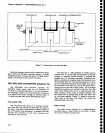
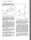
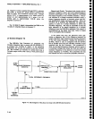
afray in
the feedback
loop
of
inverting
amplifier
ul073A.
All
of
the amptifier's
feedback
is
through
R1072
when
the
output
swings
to
the negative
limit.
As
th€
output voltage
swings
less
negative,
it
sequentially
passes
the tap-point
voltages
of a series
of
voltage
dividers
connected
b€tween
0 V
(the
summing
node
at
pin
12)
and a
negative
reference
s€t
by e1047.
lf the
ot
tput
becomes
positive
with
respect
to
a
given
divider
tap,
a corresponding
diode in
U2059 forward
biases
and
connects
the output
to
the
tap,
which
creates
addi-
tional
feedback
through
one
leg
of
the divider
to
the
summing
node.
This
causes
R2051,
then R2052,
then
R2053
(as
so
on
through
R20S6)
to
be
connected
in
parallel
with
R1072
as
the amptitier
output
becomes
le$s
negativs.
This
progressively
increases
the
feed-
back,
which
causes
the
gain
of
Ul073A
to decrease.
Another
series
of
dividers
connected
between
the
amplifier's output
and
a negative
vottage
reference.
causes
the diodes
in
U1059
to sequ€ntlalty
conduct
as
the
output
becomes
more
positive.
Resistors
R2O6O,
then
R2061,
then
R2062
(as
so on
through
R206S)
are
sequentially added
in
parallel
with
the
existing
feed-
back.
Soft
diode
turn-on
characteristics
and
a large
number of
breakpoints
result
in
smooth
gain
changes.
The
nonlinear
amplifier's
voltage-gain
characteristic
is
controlled
by the shaper
reference
voltage,
which
is
set
by
R2049.
Altering
R2049
wiil
make
the
breakpoints
either closer
together
or
further
apart;
in
practice,
this
resistor
is sel€cted
to
correct
the
tolerance variations
of
th€
18 MHz
VCO
varactor.
The
fomrard
drop
of
the shaper
diodes
gives
Ul073A
an offset
voltage.
Temperature
correction
diodes CR1086,
CR1087,
and
CR1OBB correct
this
ofiset
over
a
wide
temperature
range
by
summing
a
co.rection voltage
through
R1074.
These
diodes also
compensate for
the lack
of
s€ries
diode
drop across
R1072 and eliminate
offsets
at
the
summing
input
of
Ul0738. Selecting
R1070
provides
fine adjustment
of
the
VCO's
center
frequency.
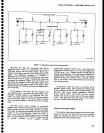
lC
U107gB
is
an inverting
amplifier
that increases
the shaper
output
voltage
swing
to
a
level
that
can control
the varactor
of
the
1g MHz
vco.
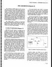
A differential
amplifier
with
weil-defined
timiting
characteristics
is
used for
the 1g
MHz VCo.
Emitter
degeneration is
Lsed
to control
loop
gain.
Transistors
02096
and
Q2087
form
the
differentiat
pair
of
transis-
tors,
with
the emitters
coupled
through
C2091.
Transformer T2092
provides
ac
feedback
for
the
collector-base
junction
of
02096 and
also
creates
the
maiority
of
the resonator
inductance.
The
total resona-
tor inductance may
b€ adjusted
by trying
different com-
binations
of
connections
between
taps on
inductor
Tl
091
and
transformer
T2092.
These
taps allow coarse
adiustment of
the VCO
center
frequency.
The
capacitor
of
the
resonator is
varactor
CR1089.
Capacitor
C10gg
7-12
complet€s
the
resonator ac
path
and
acts as
a
dc
bloc( which
allows
a bias voltage
to
be
impressed
on
the
varactor. Resistor
R2092 and
capacitor
C2090
damp
the
02096
collector,
which
prevents
high-
trequency
instability in
the
oscillator.
Translstor
Q2087
provides
a
bufiered
oscillator output.
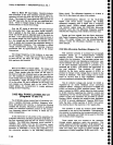
A discrete
two-stage amplifier
provides
an
unsa-
turated voltage
gain
of approximat€ly
43
dB
for
thg
18MHz
signal
lrom
the 22A0
MHz Reference
Mixer
board. Transistor Q1041 ls
the
common-emitter
first
stage
while Q1042 and
Q1043 form
the difierential
second
stage.
Th€
differential stage limits
the output
swing
to 0.8
V
to
prev€nt
over-
driving
the
following
ECL circuitry. Dc
bias
is malntained
by Q1041, which
has
dc
collsctor-base feedback via
R1O46 and
the
Rl043/R1048
vdtage
divider. Transistor
Q1043
receives its
base
bias through R1042. Each
transistor
operates
with 5
mA of
quiescent
current.
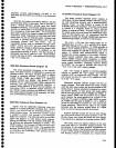
ECL line receivers
U2041D
and
U20418 amplify and
bufier
the
18 MHz
signals from
the Reference Mixer and
the
VCO,
respectively.
These
two signals are
then
applied
to
the
phase/frequency
detector
for com-
parison.
A
pair
of ECL D-type flip-flops,
U2031A
and
U20318,
comprise the
phase/frequency
detector. The
flip-flops
drive
a common
reset lins with
a
wired-AND
output.
The
clock input of
u20318
is
driven
with
the
signal from the 18MHz VCO,
and
the
clock
input of
U20314
is
driven
with
the
signalfrom
the
18 MHz
signal
from
the Referenee
Mixer.
Both flip-flops are
configured
to
r€set
together
whenever
both
are set.
lf they are
clocked
with signals
that exactly match in
trequency and
phase,
then both
flip-flops set simultaneously and
then
almost immedi-
ately reset. lf
the R€ference Mixer signal has a slight
phase
lead, U2031A
will remain set longer
than
U20318.
lf
the
Reference
Mixer signal has a
slight
phase
lag,
U20318
will set
first
and
remain set the long-
est.
The signal that
has
the
phase
lead will cause
the
associated flipflop to be
set a
grgater p€rcentag€
of
time than
the
lagging flip-flop. lf there
is a frequency
difference between
the two
inputs,
the
flip-flop with
th€
higher input frequency
will
be
set
more of the time than
the
other flip-flop, The
ratio
between
the
filtered output
signals
of
the two
flip-flops
indicates whether the
Refer-
ence Mixer
signal
leads,
lags; or
differs
in frequency
from
the
18 MHz
VCO signal.
The
outputs
of
the
flip-flops
are low-pass filtered by
Cl031
and
C1028
and applied
to differential
amplifier
U1031.
U1031
compares
the
outputs
of
the
flip-flops
and
produces
an
output
that
controls the tuning
of the
2182MHz microstrip
oscillator. The
phase-lock
loop
bandwidth is
controlled by
R1026,
C1029,
Rl027,
and
C1026.
The
gain
slope
breaks to
-l2dB/octave
for
frequencies
betow
16 kHz. Resistors R1033 and
R1034
o
o
o
a
I
o
o
a
o
a
o
a
o
o
o
o
o
o
o
o
a
o
o
a
o
o
O
o
a
t
a
o
o
o
O
o
o
O
o
o
o
o
o
O