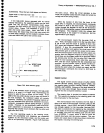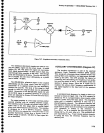
This
synthesizer
uses
a
variable
modulus
prescater
to
divide
the
VCO
frequency
before
is
processeO
by
the
"+N"
counter,
such
as
shown
in
Figure
7-29.
The
vari_
able.
modulus
prescaler
is
iontroilej
by
a
moclulus
con_
trol input.
When
the
line
is
high
tne
pr6scater
is
a
divide
by
P+l
and
when
the
tine
is
l6w
the
division
cnange"
to
P.
A common
type of.
pre.scaler
is
a
*1g1li.
A cy:crc
of
system
op€ration
starts
with
all
programmable
counters
loqOe!.1n9
*OV
to count.
The'var]able
modutus pres-
caler
initiaily
divides
by
p+1.
Two
programmable
dividers
are
used
with
this
sys-
te-T,
qoth
triggered
by
the
prescaler
output.
One
is
a
+N,
yith
N
being
a relatively
large
numbei,
tne otner
is
a "+A",
where
A
is
a
small
numOlr.
One
possible
state
includes
A
-
0.
.
The
operation
of
this
system
is
as
foilows.
The
lower
case
letters
represent
variables,
the
upper
case
!:,:t:,r"^pr-"sent
the
programmed
values.
At
the
begin_
ntng
of
-th€
cycle,
p-p1l
,
a_A,
and
n_N.
After
p+1
pulses
from
the
VCO,
one
pulse
is
applied
to
the
"a,,
and
*n'
counters
and
,,n,,'decr"".e
by 1
!3
-
t-1,
n
-
N-1).
This
continues
untita
_
0 at
which
time
the
modulus
control
line
changes
state
and
p
_
p
while
n
-
N-A.
The
counting
co-ntinues
until
n
_
O.
Both
the
nno
and
"a,'
counters
now
return
to
the
pro-
grammed
condition.
The
total
number
of
pulses
applied
from
thE
VCO
is:
Theory
of
Operailon
-
4g4Al494Ap
Service,
Vot.
1
-
The
VCO
output
is
split
by
a
resistive power
divid€r.
One output
drives
transistor
U2O5g,
w'trictr providei
f7 lAm
of
signat
output
to
the Harmonic
Mixer.
This
device
is
biased
to
a
20
mA collector
current
by
transis-
tor
Q2055.
The
other
VCO
output
drives
a low
gain
amflifier,
Q2049,
which
is
biased
by
transistor
ozdst.
Heiative
feedback,
in
the form
of
emitter
degeneration
and
lhunt
current
feedback,
sets
and
stabilizes
the
gain
to
ensure
stability
with
regards
to
spurious
oscillations.
The
out_
put
of
Q2049,
to
drive
the
variabte
modulus
prescaler
is
0 dBm.
The
variabte
modulus prescaler
tj3ost,
is
a
+92133
tC
that features
an
ECL
input
with
a
TTL
or
CMOS
compatible
output.
.
The
major
circuit
of
the
synthesizer
is
U4041,
a
large-scale-integration
CMOS
device,
which
is
used
for
frequency
synthesis
apptications
with
a
variable
modulus
prescaler.
The
device
contains
three
program-
mable
counters;
a
+N,
a
modulus
control
counter +A,
and
a
reference
divider
that
divides
an
input
from
a
cry-
stal
controlled
source
or
other
reference
trequency
down
to
a
desired
frequency.
This
device
has
a
speeO
comparable
to
TTL.
lt also
contains
a
phase-frequency
detector
which
drives
an external
toop
filter.
U+Oit
wiit
accept
data for
N,
A, and
R inputs
from
a
4-bit
data
bus
while
a
3-bit address
bus sel€cts
the information
to
be
loaded.
Data
containEd
on
instrument
bus lines
DB4
to
DB7
is
loaded
when
the enable
line
goes
high.
Address
information
is
contained
on
instrument
bus
lines
DB0,
DB1,
and
DB2.
The
appropriate
g2
latches
are
also
contained
within
this lC.
-The
output
from
ths
phase/frequency
detector
in
U404'l is
a
chaln
of
puls€
signals
at
the ieterence
fre-
quency.
The
pulses
contain
both ac
and
dc com_
ponents.
The
ac
part
of
the signal
causes
reference
sidebands
to appear
on
the
VCO
output.
These
side_
bands
are
suppressed
by
two
active
loop
filters
consist_
ing
ol
U2040A
and
U204OB. The
detector
outputs,
CR
and.
dv,
which
are
similar
but with
reversed potaritrj,
apply
differentialty
to
the
input
of
U204OA.
Stight
differences
in
pulse
width
between
the
two outputs gin-
erate
a dc
voltage.
This
is further
filtered
by
an
active
low-pass
filter,
U20408,
to suppress
frequencies
above
20 kHz.
Then
it is applied
to the varactor
diode
CR2O6g
in
the
200-220
MHz
VCO.
U2MOA
is an
integrator
with
a series
resistor
added
to the feedback
capacitor.
This
controts
the
slope
of
the loop
gain
at
gain
crossover.
To
provide
additional
suppression
of
the reference
sidebands,
an
RC
active
two
pole
filter,
U20408,
is
added.
Cutoff
frequency
is
about
20
kHz. The
loop
fitter (U2040A)
anct
the
VCO
providB
the dominant
poles
that
determine
th€
system
response,
A damping
factor
near
unity
provides
the
stability.
Additional
filtering
in
the
form
of
passive
com-
ponents,
with
a
high
frequency
cutoff,
are added
between
the output
of
U203gB
and
the varactor
diode
Ntotar
-
(p+l)A
+
p(N-A)
:
A
+
pN
Both
N and
A
are
programmable
such
that
F,"o
]
(A
+_PN)Frer.
This
leads-to
a
possible
channel
spacing
of
Fr"y,
obtained
by
changing
A
by 1.
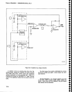
A
functional
block,
diagram
of
the
Auxiliary
Syn-
thesizer
is
shown
adjacent
to
the
schematic
in
the
diagrams
section.
The
VCO
(02071)
is
configured
in
a
Colpitts
oscillator
circuit
with
ttre lnductance
as
a
three
turn air
core
coil
with
feedback
provided
by
C2072
and
C2071.
Coarse
tuning
is
accomptistreO
witn
C1O7O,
while
the
voltage
control
of
the frequency
comes
from
the varactor
diode,
CR2O68.
This
diode
jrovides
a fre_
quency
shift
of
over
30 MHz
from
a
voitage
swing
of
+5V
to +11
V,
which
is
ampte
overtap
torine
20MHz
tuning
range,
The
output
power
of
the oscillator
is
0 dBm
into
50O.
The
oscillator
is
biased
so it
can
be
turnecf
off and
on
rapidly.
The
VCO
is
turned
off
by
turning
e2076
on.
In
operation,
the
synth€sizer
is
iurned
off
during
periods
when
information
is
presented
on
the
CRT.
Synthesis
and
counting
is
done
during
retrace
time
to
prevent
possible
interference
on
the
display
from
any
radiated
energy
from
the synthesizer.
7-81


