


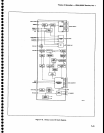
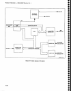

Theory
of
Operation
-
494A/494Ap
Servlce,
Vol.
1
ing sid€
ar€
through
the
parallel
combination
of
resis-
tors R4049
and
R4048
and
capacitor
C4057.
The
series
connection
of
resistor
R4049
and variable
capacitor
C4057
provides
high-frequency
respons€ compensation.
Capacitor
C2A7
controls
high-frequency
feedback.
Input
to the
non-inverting
side
is
through
resistor
R5029
to the
base of
Q4025A.
R4019 and
RS035
set
the
dc
level
for
the feedback
loop
to the
base ol
040258.
Variable
capacitor
C5021
provides
adjustment
to
set
transient
gain.
High-frequency
feedback
is con-
trolled
by capacitor
C3021.
Gain
of each
amplifier
section
is
approximately
20.
(Horizontal
deflection
sensitivity
of the crt
is approxi-
matefy
21.3Vldiv
per
side.)
Each section
is
singte-
ended
and
incorporates
a
gain-
degenerated
dual
pNp
transistor at
the input
side
(for
temperature
compensa-
tion)
connected
as a
differential
amplifier.
For
example,
Q40388 of
the right
deflection
amplifier
drives
emitter
follower
Q4047.
Signals with
a low
rate
of change
drive
the output
transistor
through R5037
and
p3033.
As
the
rate
of rise
increases,
the drop across
R5037 increases
and
when
it reaches
0.6 V, either
Q4035 or
Q4042
are
biased on.
These
transistors
provide
the
high
cunent
drive
for
the
output
transistors.
when
the signal
rate of
change
is
low,
Q1043
drives
the crt
d€flection
plate
and
e1o4g
provides
bias current
for
the amplifier.
As
the rate
of
rise increases,
C3039
couples
the
signal
to
the
base of
Q1049.
Q1049
provides
the
positive
drive
to the
deflection
plate,
and
01043
provides
the negative
drive.
Each output
transistor
can
provide
a 200 V
excursion
in
approximately
1
ps.
The
horizontal
amplifiers
operate with
approximately
1 mA
ol
bias
current
in
the output
stage, as set
by the
current
through resistor
R3031,
R1052, and
R1049
at
the base
and
emitter
of
Q1049.
Cunent
through resis-
tor
R3031 also
provides
the current
for the input
stage,
04038A/040388.
Emitter
follower
e4042, operates
at
approximately
2.5 mA.
Resistors
R104S and
R1034.
in
the emitter circuit
of
Q1049 and
el043, degenerate
the
output
stage for
fast
steps.
Current
from
the
-15
V
source
through resistor
R4033,
sets the output
operat-
ing level.
Feedback
resistor
R3045 sets
this output
level
at approximately
142
V.
Operation
of
the
right-hand
(inverting)
section
is
basically
the
same
as
th€
teft-hand (non-inverting)
sec-
tion.
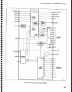
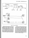
Vertical
Section
VIDEO
FILTER
OUT, from
the
Video
processor,
and
VERTICAL
SIGNAL,
from
the Digitalstorage,
are
routed
through
switch
lC
U6055A,
under control
of
the
STORAGE
OFF signal
from
the Digitat
Storage
board.
7-48
Note
that the vlDEo
FILTER
ouT
signal
ls
bufiered
by
lC
U7065 to
prevent
a change
in load
transients
from
aff€cting
th€
signal level. A
high on the
STORAGE
OFF
line
selects
the buffered
VIDEO
FILTER OUT signal,
and
a low
selects
the
VERTICAL
SIGNAL.
U6065
inverts
the selected
signal and clamps
it
to
ground.
Both
the
VIDEO
FILTER
OUT
ANd
thE VERTICAL
S]GNAL
ArE
specified
at
0.5
V/div
with
0
V
for
the baseline and
posi-
tive voltages above
the
baseline.
The signal is re-inverted and offset
by bufier
U6073
so center
screen represents 0
V. Buffer
U6073
supplies
a sample of
this
cent€red
signal
to the
rear-panel
VERT
OUT
connector
via
edge connector
pin
46.
The output
of
U6073
is also applied
through
switch
U60558, when
the R/O OFF line is
high,
to the vertical shaper
circuit.
When R/O
OFF
line is
low,
the VERTICAL R/O
signal is
applied
to
th€
shaper.
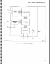
The
vertical
section
shaper
(R4062,
R4065, R4067,
R4069,
R4064, and
CR4063, CR4064,
plus
the
preamplifier
U20621operates
the
same
as
the
horizontal
section.
Q4078 limits
positive
Excursions
to
approxi-
mately one
division
above the top of
the
scr€en
to
pro-
tect the
output stages
from
being
overdriven.
The
vertical
output
stages are similar
to the
horizon-
tal
stages, with the
€xception of higher bias current.
Current
flow
of
approximately
1 mA, through resistors
R3089
and R3098,
produces
approximately
5
mA in
the
output stag€s.
To
correct
for the
increased current
in
the dual input stage
transistors, Q408il
and
Q4101,
resistors R5081 and
R5099
are
lower value than
their
counterparts
R5041 and R5027
in
the horizontal
amplifier.
U6024 compares
the signal
level from
the baseline
clamp,
U6065,
with
a
reference l€vel set by divider
R7032/R7034.
This
produces
the CLIP
signal for
the
Z-Axis
interfac€ circuits. When the
VIDEO FILTER
OUT
signal is rnore negative than
the reference
level
(approximately
1
division
above
baseline),
it
pulls
the
CLIP
line low.
R7021
pulls
the CLIP
line high if
the sig-
nal
is more
positive
than
th€
reference level.
Z-AXIS AND
RF INTERFACE
(DTAGRAM
28)
The Z-Axis and RF
Interface board
contains the
RF
interface circuits,
crt
Z-axis drive
circuits,
power
moni-
tor
circuits,
and
a timer that
measures
operational
hours. This
board
provides
beam
intensity
(nominally
from
the
front
panel),
baseline
clipping. and
unblanking
logic for
the
signals
or readout data.
Unblanking
logic
comes from
the Sweep
board, the
Crt
Readout,
the
Deflection Amplifiers,
and
the
Digital
Storage.
The
RF
Interface
circuits
receive data
from
the
microcomputer
that
controls
the
RF Attenuation, transfer
switch,
and lF
selection. A
power
fail
circuit on
the board detects
any
o
o
a
?
o
I
a
o
o
)
a
o
t
o
o
o
I
I
I
o
o
a
o
a
o
o
t
o
a
o
I
o
a
o
I
o
o
o
I
o
o
o
o
o