


Theory of
Operaton
-
4g4A/4g4Ap
Service,
Vol.
1
to
lock
the
difference
trequency
from
th€
Harmonic
Mixer
to
25
MHz.
The
phase/frequency
detector output
is a voltage
that is
proportional
to the
phase
difierence
between
the
25
MHz refer€nce
and
the
lF
signal from
the
g29
MHz
Harmonic
Mixer.
This
correction
voltage
is
then applied
to
the
719
MHz
VCO
to lock
it
to
the
reference.
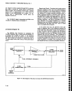
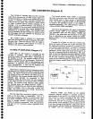
The
detector
circuit
consists
of
two D-type
flip-flops,
U2U7A and
U2047B,
and
a
differentiat
ariiptifiei
stage
used
as
a
NAND-gate
(U1044A).
The 25
MHz
referenie
signal, from
the frequency
divider, is apptied
to
the
cfock input
of
flip-flop
U204tA;
the
nominat
25
MHz
sig-
nal
from
the
829
MHz
Harmonic
Mixer is
applied
to the
clock
input
of flip-flop
V204ZB.
The
rising
€dg€
of
the
input
signal
to each
flip-flop
causes
the
e(bar)
outputs
to
return
to
the
low
level
only
after
both
flip-flops
have
been
clocked.
lf
the
frequency
out
of
the
g2g
MHz Harmonic
Mixer
is
below 25 MHz,
or
if its
phase
lags
that of
the 25
MHz
reference,
the
Q(bar)
output
of
ftip-flop
U2047A
witl
remain
high
longer
than
the
a
(ba0
output
ot
u20478.
lf
the
frequency
out
of
the
Harmonic
Mixer
is
above
25 MHz,
or
if its
phase
leads,
the
opposite
will
occur.
When
the
two
flip-flops
are clocked
at
the same
fre-
quency
and
phase,
the
two outputs
will
be high
for
the
sam€
amount
of
time.
The
e(bar)
outputs
are
applied
to a compensation
or
differential
amplifier
U3059,
that
determines which
output
is high
for
the
longer
time.
Compensation
amplifier
Ug05g
provides
part
of
the
loop
gain
to ensure
that
the 719 MHz
oscillator
will
track
the sweep
of
the
2192
MHz
reference
oscillator.
The compensation
amplifier
also
limits
the loop
bandwidth to 100
kHz
to make
certain
that the loop
wilf
not oscillate.
Note
the
differential
inputs
to the
amplifier
each
include
a
low-pass
RC filter
to attenuate
the
undesired
high
frequency
clock
pulses
from
the
phase/frequency
detector.
The nominal
swing of
the U3053 output
is
from
+12V
to
-12V.
Since the
compensation
amptifier
is
capable of
considerably
more
output
than is
needed
to
control
the
oscillator,
a voltage
divider is
used
to limit
the output
and reduce amplifier related
noise.
This
vol-
tage
divider, consisting
of
resistors
R2053,
R2054,
R3051, and
R3052, reduces
the
possible
*12V
swing
to
+5
V
to
+12
V,
as
reguired
by varactor
diode
CR1011. Nominalvoltage
swing in a
locked condition
is
+6.75
to
+7.5 V.
Thus,
dependent
upon
whether
the
Harmonic
Mixer
frequency
is above or
below 25
MHz,
the correction voltage swing,
applied
to
diode CR1011,
is
more than nominal
to
correct
the
oscillator
frequency.
2nd Local
Oscillator
Oupuf Circult A
portion
of
each
2nd
LO
output signal is
sent
to the
front
panel
2nd
LO
OUT connector. This output
provides
signal
for
external
accessory
equipment,
such
as a
tracking
gen-
erator. Each
local oseillator
(719
MHz and
2182 MHz)
output is applied
through
power
dividers
to
a
power
combiner
for application
to th€
2nd LO
OUT
connector.
The 719 MHz
oscillator
frequency
is applied
from a
power
splitter
(R3027,
R3028, R3029)
through
a
1
GHz
fow-pass filter
(C3025,
C2024, C1023. C1021
,
and
three
printed
inductors),
to
the
power
combiner
(R2024,
R2025,
R2026),
and
the
front
panel
2nd LO
OUTPUT.
The 2182 MHz oscillator signal is applied
through a
power
splitter
(R1021,
R1022, R1023), a 2.2
GHz
band-
pass
filter
(consisting
of
coupled
1/4 wavelength
printed
lines)
to
the
power
divider
(R2024,
R2025, R2026)
and
the front
panel
2nd LO OUTPUT.
Both 2nd local oscillator signals,
2182MHz
and
719MHz, are
present
at
the
front
panel
when
the
829
MHz
2nd
Converter
is
selected.
719 MHz
Output Clrcult
The 719 MHz
2nd Local
Oscillator signal is applied is applied
through divider
resistors
R2021, R2023,
and R2A24
to isolation
amplilier
Q2021. 02021 boosts th€
signal level from
about
0 dBm
to
+12
dBm to drive the 829
MHz mixer.
The output
of the
amplifier includes a
3 dB
attenuator
(consisting
of resistors
R2027, R2028,
and
R2029),
to
ensur€
a
50
ohms
non-r€flective
source impedance.
The signal level at
test
point
J2026
is
typically
-6
dBm.
o
o
o
o
t
a
t
a
o
a
o
I
o
o
o
O
o
o
o
o
a
a
o
o
o
o
o
O
t
,
a
O
o
o
o
o
a
a
o
o
a
o
o
o
7-18