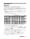
Note
The on-screen amplitude level will probably not change as expected, since the
video circuitry is assumed to be faulty.
15. Monitor
ASTP14
while stepping the reference level from -10
dBm
to j-30
dBm.
If the
voltage does not step approximately 100
mV
per 10 dB step, refer to “Video MUX” in
this chapter.
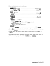
16. If the Video MUX is working properly, monitor
A3TP15
with the oscilloscope and step
the reference level from -10
dBm
to
+30
dBm.
If the voltage does not change 100
mV
per 10 dB step, refer to “Video Filter” in this chapter.
17. If the voltage at
A3TP15
is correct, move the oscilloscope probe to
A3TP17
and step the
reference level between -10
dBm
and i-30
dBm.
If the voltage does not change 100
mV
per 10 dB step, refer to “Video Filter Buffer Amplifier” in this chapter.
18. If the voltage at
A3TP17
is correct, move the oscilloscope probe to
A3TP6.
Set the
following controls to keep the ADC MUX set to the MOD-VIDEO input during the
sweep
:
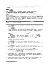
Sweep time . . . . . . . . . . . . . . . . . . . . . . . . . . . . . . . . . . . . . . . . . . . . . . . . . . . . . . . 50 s
Detector mode . . . . . . . . . . . . . . . . . . . . . . . . . . . . . . . . . . . . . . . . . . . . . . . . . Sample
19. Step the reference level from -10
dBm
to i-30
dBm
while monitoring the voltage change
on the oscilloscope. If the voltage does not change 100
mV
per 10 dB step, refer to “ADC
MUX” in this chapter.
20. If the voltage at
A3TP6
is correct, move the oscilloscope probe to
A3TP8
and step the
reference level between -10
dBm
and i-30
dBm.
If the voltage at
A3TP8
is not the same
as that at
A3TP6,
replace
A3UllO.
21. If the voltage at
A3TP8
and
A3TP6
are equal, move the oscilloscope probe to
A3TP7.
22. Change the reference level from -10
dBm
to 0
dBm.
The voltage change on
A3TP7
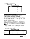
should be between 630
mV
and 770
mV.
If the voltage change is outside of these limits,
refer to “Variable Gain Amplifier (VGA)” in this chapter. The gain of the VGA should be
7
&lo%.
Log
Offset/Log
Expand
Refer to function block X of A3 Interface Assembly Schematic Diagram in the
HP 8560 E-Series Spectrum Analyzer Component Level Information.
The log scales are modified using a combination of amplification and digital trace
manipulation. The video input to the A3 assembly is either 10 dB/div or linear. To obtain
the 5 dB/div scale, the CPU manipulates the trace data from the 10 dB/div scale. To obtain
the 2 dB/div scale, the video signal is amplified and offset so that top-screen in 10 dB/div
corresponds to top-screen in 2
dB/d
iv. To obtain the 1 dB/div scale, the CPU manipulates
trace data from the 2 dB/div scale.
In 2
dB/div,
Log Offset/Log Expand amplifies the top 20 dB of the display. This is done by
offsetting the video signal by -0.8 V and providing a gain of 5 to the top 0.2 V of the video
signal. The -0.8 V offset is accomplished by sinking 2
mA
through R114 by current source
U105/QlOl.
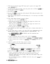
I. On the spectrum analyzer, press
(PRESET),
ISPAN),
ZERO
SPAN, (CAL), and IF
BDJ
IIFF
.
ADC/lnterface
Section 8-15


