YTF
Driver
Circuit
The YTF driver circuitry consists of the Sweep + Tune Multiplier, FAV (Frequency Analog
Voltage) Generator, YTF Gain and Offset, and YTF Drive. Refer to function blocks Q, R,
S, and T on Al4 Frequency Control Schematic Diagram (sheet 3 of 5). The FAV Generator
generates the 0.5
V/GHz
signal. The YTF driver circuitry can be half-split by checking the
rear panel 0.5
V/GHz
output.
Note
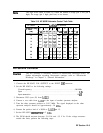
The rear-panel output changes according to the external-mixer mode selected.
The preselected external-mixer mode must not be selected while executing this
procedure.
The Sweep + Tune Multiplier takes tune information (YTO start frequency) and sweep (based
on LO span) and multiplies it so that it is correct for the appropriate YTF band.
C31
of the FAV Generator holds the YTF steady during retraces between multiband sweeps.
Switch U415C and R94 provide the YTF de-hysteresis pulse. A de-hysteresis pulse is activated
at the end of spans greater than 1 MHz. In high band, amplifier U402A provides an offset
voltage to account for the 310.7 MHz offset (U415A open) between the desired harmonic of
the YTO frequency and the center frequency. In low band, switch U415A is closed to account
for the 3.9107 GHz first IF offset between the YTO frequency and the center frequency. This
signal is 0.5
V/GHz
of tuned frequency and is available at the rear panel.
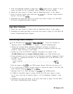
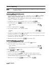
1. On the HP 85623, press (PRESET), and set the controls to the following settings:
Start frequency . . . . . . . . . . . . . . . . . . . . . . . . . . . . . . . . . . . . . . . . . . . . . . . . . 0 Hz
Stop frequency . . . . . . . . . . . . . . . . . . . . . . . . . . . . . . . . . . . . . . . . . . . . . . 13.2 GHz
2. On the HP 85623, press
[AUXCTRL),
REAR
PEEL
, and
.5
V/G&r
EFAV)
.
3. Monitor the signal from the rear-panel LO SWP
1
FAV OUTPUT connector with an
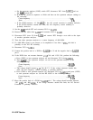
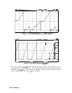
oscilloscope. The waveform should resemble Figure 12-4.
4. Set the spectrum analyzer controls as follows:
Start frequency . . . . . . . . . . . . . . . . . . . . . . . . . . . . . . . . . . . . . . . . . . . . . ...8 GHz
Stop frequency . . . . . . . . . . . . . . . . . . . . . . . . . . . . . . . . . . . . . . . . . . . . . . ..lO GHz
5. Monitor A14J15 pin 1 with an oscilloscope. The waveform should resemble Figure 12-5.
6. If the ramp is not correct, confirm the operation of the Main Coil Tune DAC and Sweep
Generator. Refer to “Unlocked YTO PLL” steps 36 through 40 and “Sweep Generator
Circuit” in Chapter 11, “Synthesizer Section.”
7.
Set the HP 85623 to the following settings:
Centerfrequency . . . . . . . . . . . . . . . . . . . . . . . . . . . . . . . . . . . . . . . . . . . . . ...5 GHz
Span . . . . . . . . . . . . . . . . . . . . . . . . . . . . . . . . . . . . . . . . . . . . . . . . . . . . . . . . . . . . OHz
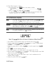
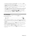
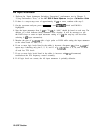
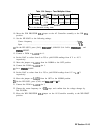
8. Monitor A14J15 pin 3 with a DVM. For a center frequency of 5 GHz, the voltage should
measure -1.33 Vdc f0.2 Vdc. Use the following formula to calculate the voltage:
v(J15
pin 3)
=
-yizv
(freq in GHz)
-
0.078 V
RF Section 12-13


