


9. On the HP 85623, press
(-1,
ICAL),
IF
BDJ
OFF, M#m
I
OF
2, and
FLA’F#ESS
.
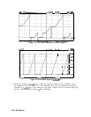
Increase the gain of the flatness compensation amplifiers to maximum by entering 0
using the data keys. This sets the gains in the flatness compensation amplifiers to their
maximum values.
10. Connect the other spectrum analyzer to A15J601 and measure the 10.7 MHz IF signal
level. The signal should measure greater than -10
dBm.
If the signal level is incorrect,
continue with step 13.
11. Enter 4095 into the HP 85623 Flatness Data. The signal level at A15J601 should measure
less than -36
dBm.
This sets the gain of flatness compensation amplifiers to a minimum.
If the signal level is incorrect, continue with step 13.
12. Check that the gain stages are properly biased and functioning.
13. Check the attenuator stages and flatness compensation control circuitry.
a. For minimum gain (flatness data equals 4095), RF GAIN (A15U909 pin 10) should be
at -1.6 Vdc and the current through each section as measured across R667 or R668
should be about 7 mA.
b. For maximum gain (flatness data equals 0), RF GAIN (A15U909 pin 10) should be at
approximately 0 Vdc and the current through each attenuator section should be close
to 0 mA.
Caution
As long as the flatness data just entered is not stored, the previously-stored
flatness data will be present after the power is cycled.
14. Move the A2 controller assembly WR PROT/WR ENA jumper to the WR PROT
position.
15. Reconnect the cable to A15J801.
Flatness
Compensation
Control
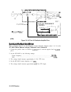
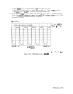
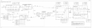
Refer to function block G on Al5 RF Section Schematic Diagram (sheet 1 of 4) in the
HP 8560 E-Series Spectrum Analyzer Component Level Information.
The Flatness Compensation Control consists of a buffer amp (U909C) and two identical
voltage-to-current converters (U909B and U909D). The thermistor RT901 in the buffer amp
provides temperature compensation for the PIN diodes in the gain stages and the SAW filters.
The gain of the Flatness Compensation Amplifiers is driven to a minimum by the REDIR line
going low during Automatic IF Adjustment.
Control
Latches
Refer to function block H on Al5 RF Section Schematic Diagram (sheet 1 of 4) in the
HP 8560 E-Series Spectrum Analyzer Component Level Information.
The control latches control the PIN Switch Drivers illustrated in Function Block I.
1. Connect the positive lead of a DVM to A15J901 pin 15 (HEXTMIX). Connect the
negative lead to A15J901 pin 6. The measured signal controls the switching between
internal and external IF signals.
12-18 RF Section