


16-Bit
Post-Trigger
Counter
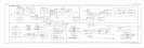
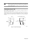
Refer to function block E of the Al6 fast ADC assembly schematic diagram in the
HP 8560 E-Series Spectrum Analyzer Component Level Information. The 16-bit post-trigger
counter controls the number of static RAM memory locations that will be written after the
trigger occurs. This counter consists of U19, U20, U21, U22, and U47. The counter is loaded
from the CPU on the A2 controller assembly when the Al6 fast ADC assembly is in “read”
mode. The CPU loads the counter by first setting the LLOADPOST (bit 7 of the fast ADC
control word) and the LREADCLK (bit 9 of the fast ADC control word) to their low state.
The CPU then writes the 16-bit word to the fast ADC secondary address. The rising edge of
PCLK then latches the 16-bit data into the post-trigger counter.
The post-trigger counter begins counting upward in “write” mode on the first rising edge of
PCLK after the LCOUNT signal from the trigger circuit goes low. The frequency of PCLK is
the programmed sample rate. When the post-trigger counter reaches its terminal count, the
LSTOP signal goes low and disables the static RAM address counter from further counting.
LSTOP also forces LCOUNT high in NAND gate
UllD,
which disables the post-trigger
counter.
15-Bit
(32
K)
Circular
Address
Counter
Refer to function block G of the Al6 fast ADC assembly schematic diagram in the
HP 8560 E-Series Spectrum Analyzer Component Level Information.
This 15-bit programmable circular counter provides the address lines of the static RAM
(U32). The counter consists of U23, U24, U25, and U26. It counts upward from 0 to 32767
and then back to 0 in a circular fashion. When a trigger occurs, latches U27 and U28 latch
the current static RAM address so that the CPU on the A2 controller assembly can later read
the latches and determine the static RAM address of the sample that was taken when the
trigger occurred.
The CPU loads the address counter during “read” mode by first setting LLOADADDR (bit 6
of the fast ADC control word) and LREADCLK (bit 9 of the fast ADC control word) to their
low state. The CPU then writes the 16-bit load value to the CPU secondary address. The
rising edge of ACLK then latches the 16-bit data into the address counter.
After the address counter is loaded by the CPU during “read” mode, the static RAM is read
by the CPU. The RAM is read by first setting LREADMEM (bit 10 of the fast ADC control
word) and LREADCLK (bit 9 of the fast ADC control word) to their low state. Since the
LREADCLK control bit is low, a negative-going pulse on the ACLK line will occur on every
static RAM “read” by the CPU. This causes the address counter to increment at the end of
each static RAM “read” so that the address counter automatically post-increments to the
next address of RAM U32. In order for this address post-increment to occur, the LSTOP
count enable signal from the post-trigger counter must be high. LSTOP goes low when
the post-trigger counter reaches its terminal count in the “write” mode to stop the address
counter from counting. When the fast ADC assembly is changed from “write” mode to “read”
mode, LSTOP will be low. So the CPU on the A2 controller board must always first program
the post-trigger counter to a value other than the terminal count (65535) to force LSTOP
high.
8-38
ADC/lnterface
Section