


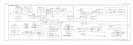
Al6 Assembly Fast ADC Control Circuits (Option 007)
The fast ADC control circuits consist of the CPU interface and control registers, the reference
clock, a clock and sample rate generator, a trigger circuit, a 16-bit post-trigger counter, a
15-bit circular address counter, a video trigger comparator, and the reference and power
supply circuits.
CPU
Interface
and
Control
Registers
Refer to function block A of the Al6 fast ADC assembly schematic diagram in the
HP 8560 E-Series Spectrum Analyzer Component Level Information.
The Al6 assembly digital interface to the A2 controller assembly consists of an 8-bit
bi-directional data bus, one address line, a most-significant byte strobe, and a least-significant
byte strobe.
The Al6 fast ADC assembly can be accessed by firmware (on the A2 controller assembly) at
two logical addresses. When the address line (ADDR3)
is
1
ow, the primary address is selected.
When the ADDR3 is high, the secondary address is selected. The data transfers between the
Al6 fast ADC assembly and the A2 controller assembly are clocked by the two strobe lines,
MSB-STRB
and
LSB-STRB.
16-bit word transfers occur as two sequential byte transfers;
the most-significant byte first, followed by the least-significant byte. The primary address
(ADDR3 low) contains the 16-bit control word written by the firmware on the A2 controller
assembly. The secondary address (ADDR3 high) supports both 8-bit byte and 16-bit word
reads and writes. There is no read/write line on the Al6 fast ADC assembly to control the
direction of data transfer. The fast ADC is
preconfigured
to read or write by setting the
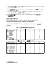
appropriate bits in the 16-bit control word. Refer to Table 8-13. If the control word is not
correct, it may result in a bus conflict.
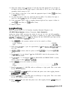
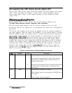
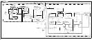
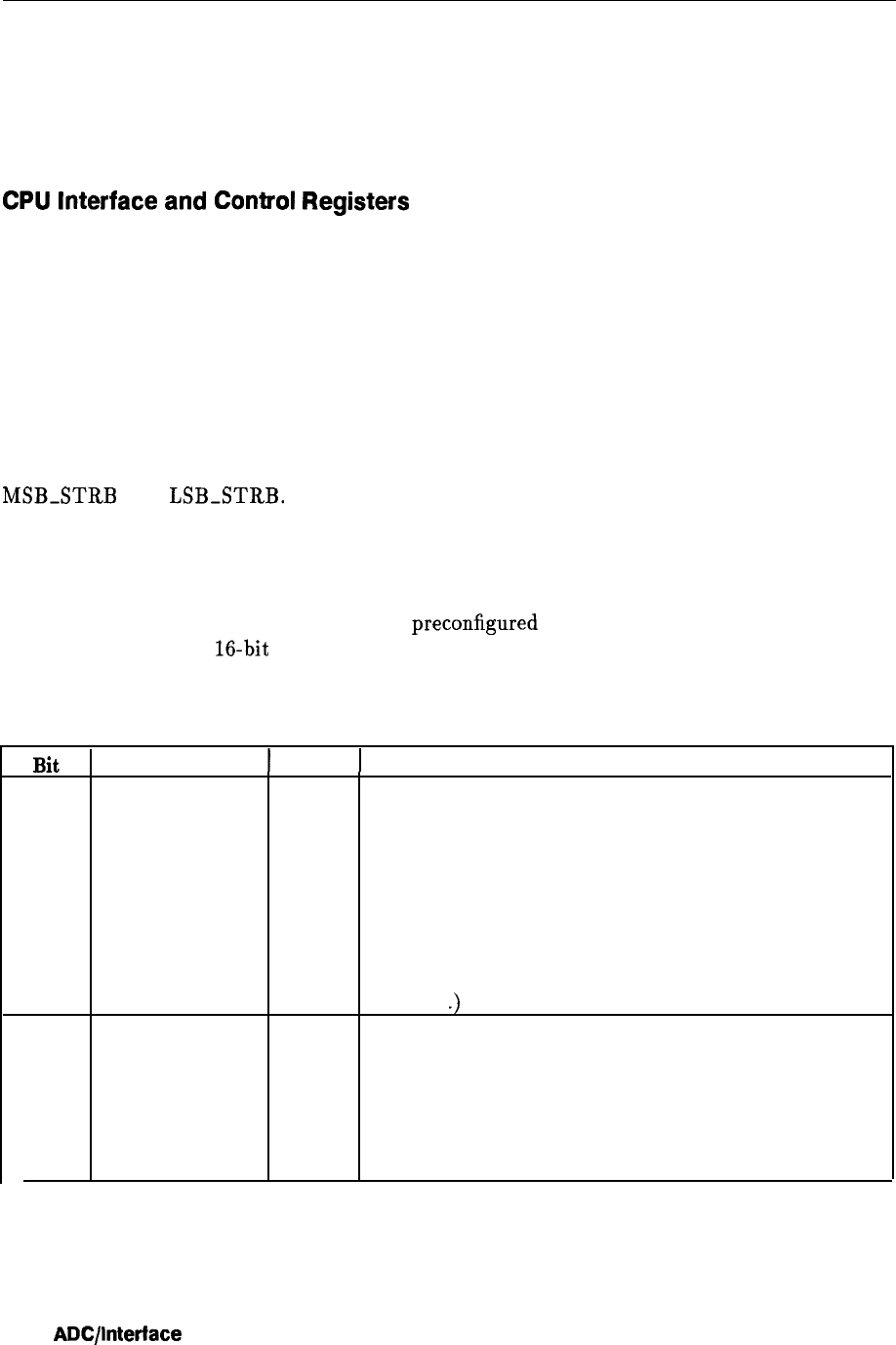
Table 8-13. Control Word at Primary Address (U3 and U4)
Mnemonic
WRITE
Bit 0
State
Description
Allows samples to be written to FADC memory.
1
All on-board clocks running and samples being written to
FADC memory. (FADC memory cannot be read by A2
controller in this mode.)
Bit 1 ARM
0
All on-board clocks turned off and no samples being written
to FADC memory. (FADC memory can be read by A2
controller
.)
Arms the FADC assembly for a trigger.
1
FADC assembly armed to accept trigger from HSWP line or
video trigger.
0
FADC assembly cannot be triggered.
8-34
ADC/lntertace
Section