


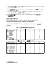
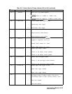
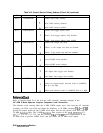
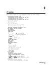
Table 8-13. Control Word at Primary Address (U3 and U4) (continued)
Bit
Bit 10
Bit 11
LREADADDR
Bit 12
LRATELATCH
Bit 13
LRLSHSWP
Bit 14
LLOADTRIG
Bit 15
LPEAK
Mnemonic
LREADMEM
State
Description
Enables read FADC memory.
Read FADC memory disabled.
Read FADC memory enabled.
Enables read trigger address latch.
“Reads” from trigger address latch disabled.
“Reads” from trigger address latch enabled.
Enables load sample rate latch.
“Writes” to the sample rate latch are disabled.
“Writes” to the sample rate latch are enabled.
Releases HSWP strobe.
Release HSWP strobe disabled.
Release HSWP strobe enabled.
Enables load video trigger level.
Load digital video trigger level disabled.
Load digital video trigger level enabled.
Peak/pit detection mode control.
Enables pit (negative-peak) detection mode if LSAMPLE
(Bit 4) is also high.
Enables peak detection mode if LSAMPLE (Bit 4) is high.
Reference
Clock
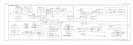
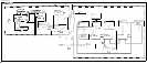
Refer to function block B of the Al6 fast ADC assembly schematic diagram in the
HP 8560 E-Series Spectrum Analyzer Component Level Information.
The reference clock circuitry takes the 8 MHz CMOS square wave clock from the A2 controller
assembly (via W59, coax 839) and triples the frequency to 24 MHz. Inverters U5A and
U5B
provide the proper match for the 8 MHz clock input, and also the desired drive level into the
24 MHz
bandpass
filter. The 24 MHz
bandpass
filter consists of R5, C8,
Ll,
C9, ClO, L2,
Cll,
L3, C12, L4, C13, C14, and R6. Inverters U6A and
U6B
provide amplification of the
24 MHz clock to produce CMOS levels, and also buffer the 24 MHz clock output.
8-38
ADC/lnterface
Section