


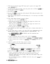
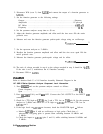
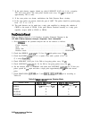
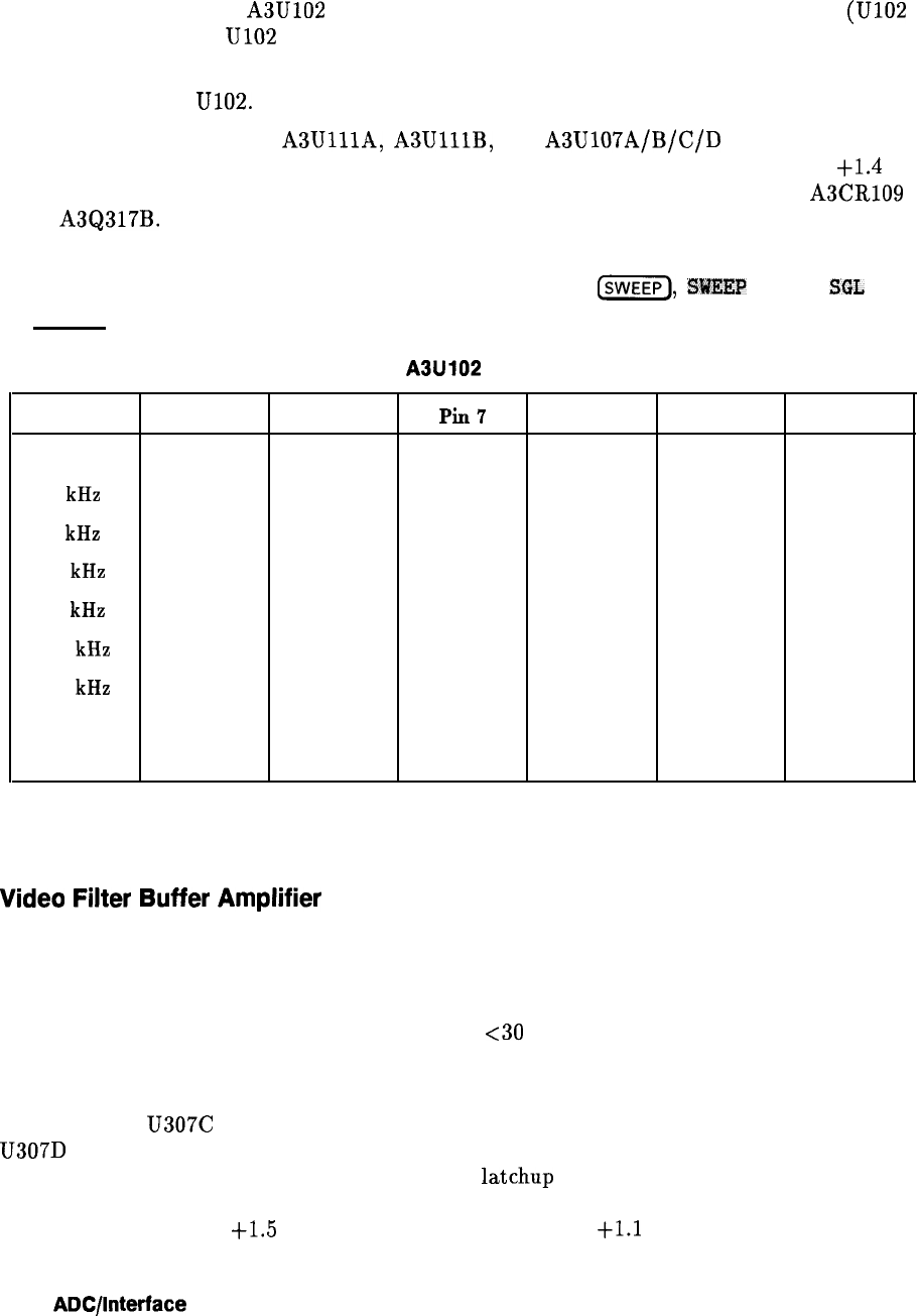
5. Refer to Table 8-7 and check for correct latched levels for the selected video bandwidth
setting.
6. If the output of latch A3U102 is not correct, trigger an oscilloscope on LLOG-STB (U102
pin 9) and monitor U102 pin 1 and other latch inputs while changing the video bandwidth.
7. If the inputs are incorrect, troubleshoot the analog bus. Correct inputs with bad outputs
indicate a faulty U102.
8. Check that the outputs of
A3UlllA,
A3UlllB,
and
A3U107A/B/C/D
are correct for
their inputs. The outputs should be high with noninverting inputs higher than the
t1.4
V
threshold voltage. If a voltage drop is noticed across these components, suspect A3CR109
or A3Q317B. Since no dc current flows through any of the series resistances or FETS
(drain to source), no voltage drops should occur.
9. To return the spectrum analyzer to automatic sweep, press
(SWEEP),
SWEEP
CONT
SGL
or
(PRESET).
Table 8-7. A3U102 Latch Outputs
Video BW Pin2
Pin 5
PiIl7
Pin 10
Pin 12
Pin 15
300 Hz
H
L L L
L
L
1
kHz
L L
L
L L
H
3
kHz
L
H
L L
L
L
10
kHz
L L L L
H
L
30
kHz
H
L H L
L
L
100
kHz
L
L
H L
L
H
300
kHz
L H
H
L
L
L
1 MHz
L
L
H
L
H
L
3 MHz
L
L L
H
L
L
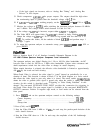
Video
Filter
Buffer
Amplifier
Refer to function block W of A3 Interface Assembly Schematic Diagram in the
HP 8560 E-Series Spectrum Analyzer Component Level Information.
The video filter buffer amplifier provides outputs for video trigger, positive and negative
peak detectors, and the analog zero-span (sweeps
<30
ms). The zero-span video
output is terminated in 500 ohms on the A2 Controller assembly. The amplifier is a
high-input-impedance buffer amplifier with a gain of one when properly terminated.
Current source U307C provides twice the current of Q316. Resistor R145 and current source
U307D shift the dc level. Resistor R260 terminates the peak detector inputs in 500 ohms. The
unterminated gain is 1.1. Diode CR114 prevents
latchup
during positive overdrive conditions
while CR113 protects Q318 during overdrive. Diode CR117 is a 12.7 V zener that limits the
peak detector output to
t1.5
V. Typically, limiting occurs at
t1.1
V.
8-18
ADC/lnterface
Section