


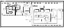
Clock
and
Sample
Rate
Generator
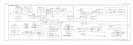
Refer to function block C of the Al6 fast ADC assembly schematic diagram in the
HP 8560 E-Series Spectrum Analyzer Component Level Information.
The clock and sample rate generator takes the 24 MHz reference clock signal and generates all
of the various clock signals used on the Al6 fast ADC assembly. The sample rate generator
consists of CMOS latch U15, CMOS counters U14 and U16, and CMOS flip-flops U7B and
U9A. The sample rate generator only controls the rate at which the static RAM address
counter (l&bit circular address counter) and the 16-bit post-trigger counter are clocked
(ACLK and PCLK respectively). The sample rate generator also controls the number of
flash ADC samples taken per bucket. The range of the sample rate is 1 sample per bucket
(12 MHz rate) to 256 samples per bucket (less than 12 MHz rate). SCLK-1 is an input to
PAL
Ul
(block A) and affects the
LP/Q
signal to ensure that the first sample of a bucket is
always clocked into latch
U30
(block J) and written into static RAM U32 (block K) when the
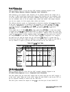
detection mode is peak or pit and the sample rate is less than 12 MHz. Refer to Table 8-12,
LP/Q
Truth Table in this chapter.
Trigger
Refer to function block D of the Al6 fast ADC assembly schematic diagram in the
HP 8560 E-Series Spectrum Analyzer Component Level Information.
When the Al6 fast ADC is triggered, the current static RAM address is latched into trigger
address latches U27 and U28 (block G), and the post-trigger counter (U19, U20, U21, U22,
and U47) begins counting. Samples continue to be written to consecutive addresses in RAM
U32 until the post-trigger counter reaches its terminal count. The CPU on the A2 controller
assembly monitors the HSWP line and starts a software timer when HSWP goes high after
being triggered. The software timer is set to slightly longer than the post-trigger counter will
be counting, so at the end of the “time-out,” the post-trigger counter has already reached its
terminal count. At the end of this “time-out,” the CPU on the A2 controller assembly takes
the fast ADC out of “write” mode and reads latches U27 and U28 to determine the static
RAM address of the sample that was taken when the trigger occurred. The CPU then writes
the trigger address (read at
U27/U28)
to the fast ADC static RAM address counter (15-bit
circular address counter). If pre-trigger or post-trigger (delay) is being used, the CPU adds or
subtracts appropriately and writes the “adjusted” trigger address to the static RAM counter.
The CPU then begins reading the fast ADC data, starting from the trigger (or offset trigger)
address.
The trigger circuitry is enabled by the ARM signal (bit 1 of the fast ADC control word).
Once a trigger occurs, the fast ADC cannot be triggered again until the ARM line goes low
(disarmed), then high again (armed).
The fast ADC is triggered by the HSWP
1
ine in
FREE
RUN
, LINE, and
EXTEZNE
trigger
modes. When
83DEO
trigger is being used, a synchronous digital video trigger signal, VCLK,
is generated by PAL
Ul
(block A) and U17A (block D).
ADC/lnterface
Section 8-37