


Theory of Operation
2715 Spectrum Analyzer Service Manual
3-43
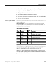
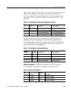
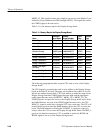
POS1. This bit, along with the HLF/F LL_L bit (called POS 0 on the schematics)
in Mode Control Register 1, determines the position on the CRT for the
B,C--Save A display. The Normal Mode does not use this bit. Table 3--4 gives
the positions on the screen that are available when using the HLF/FLL_L and
POS1 bits.
Table 3- 4: Truth Table for the B,C- Save A Display Screen Offset
POS1
POS0
(HLF/FLL_L)
Normal Mode Enhanced Mode
0 0 TOP (vertical position 245) TOP (vertical position 245)
0 1 MIDDLE (vertical position 125) MIDDLE (vertical position 125)
1 0 TOP (vertical position 245) BOTTOM (vertical position 5)
1 1 MIDDLE (vertical position 125) BOTTOM (vertical position 0)
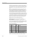
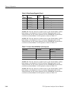
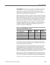
ACQM0. This bit, along with the PEAKDIS_L bit (called ACQM1 on the
schematics) in Mode Control Register 1, determines the acquisition mode
currently being used to update the waveform memory. The Normal Mode does
not use this bit. Table 3--5 gives the acquisition modes that are available when
using the PEAKDIS_L and ACQM0 bits.
Table 3- 5: Truth Table for the Acquisition Modes
ACQM1
(PEAKDIS_L)
ACQM0 Normal Mode Enhanced Mode
0 0 Max Peak Acquisition Max Peak Acquisition
0 1 Max Peak Acquisition Minimum Peak Acquisition
1 0 Min/Max Peak Acquisition Min/Max Acquisition
1 1 Min/Max Peak Acquisition Sample Acquisition
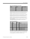
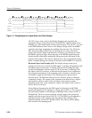
Marker/Save Register. The Marker/Save Register is located in I/O space, at
location 0x0FA01. The Marker/Save Register is a read/write register.
Table 3- 6: Mode Control Register 2
Bit
Number
Mnemonic
Activity
Level
Description
7 MKRWFM3 Low Markers on Display D
6 MKRWFM2 Low Markers on Display C
5 MKRWFM1 Low Markers on Display B