


Theory of Operation
3-30
2715 Spectrum Analyzer Service Manual
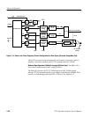
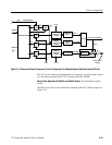
FSTROBE
FM
Main
Main
DAC
SWP
DAC
DIG
1st LO Beat to
Counter for Lock
V erification
Phase Gate
Harm Gen
VCO Module
(Strobe Gen)
Summing
and Fixed
Scaling
VREF
1st LO
1st LO to 1st Converter
N-F Strobe
PLL
DAC
VREF
DIG
Microprocessor
Serial Out
Serial In
FM
DAC
DIG
Main Coil
Driver
Summing
and Fixed
Scaling
DIG
1st LO
VREF
DIG
Decade
Atten
Analog Sweep In
Lock Limits
Comparator
Error Amp &
Loop Filter
Phase
Error
Voltage
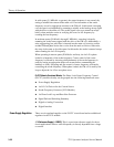
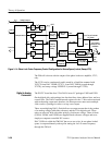
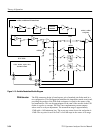
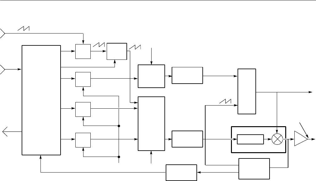
Figure 3- 14: Phase Lock Center Fr equency Control Configuration for Narrow Spans ( Locked, Sweep VCO)
The FM coil is driven with the output of the phase lock error amplifier, U713,
only.
The VCO is active continuously and is tuned by a fixed bias summed with
VCFCU from DAC U950B, VCFC L from DAC U850A (routed through
U757D), and sweep voltage VSWP PLL (routed through U757B).
The PLCFC board has four 12 bit DACs in two IC packages, U850 and U950.
On the digital side, each package has four data lines, three address lines, and two
control lines. The DACs contain internal registers for the 12 bit words associated
with each analog output and, therefore, the microprocessor must write multiple
4 bit words to a package in order to set up a new output.
These are multiplying DACs. Each delivers an output current that is the product
of an analog voltage (called the reference) and the 12 bit digital word. These
units can correctly deal with either polarity of reference voltage. Three of them
(U850A, U950A, and U950B) are supplied fixed reference voltages and serve
simply as computer controlled DC sources.
DAC U850A is called the FM DAC but serves two roles. In non phase locked
spans, its output ultimately ends up fine tuning the 1st LO center frequency
through the FM coil.
Digital to Analog
Conversion