


Theory of Operation
3-50
2715 Spectrum Analyzer Service Manual
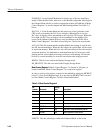
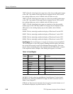
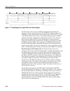
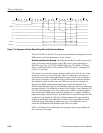
BCLK
BA<19.0>
WR_L
UPREQ
PORTVEC
UPGRNT_L
WRDATE N
0ns 500ns 1000ns 1500ns 2000ns 2500ns 3000ns
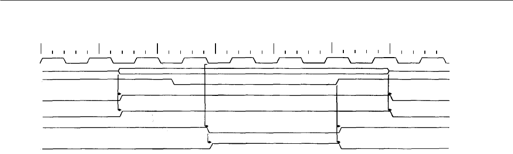
Figure 3- 17: Timing Diagram for a Typical Write to the Control Register
The CPU starts a write cycle to the Display Storage board, presenting the
appropriate address for the desired port. The PORTVEC signal becomes active,
enabling one of the enable inputs on both of the decoders, U16 and U17. As soon
as the RAM arbitrator allows access to the Display Storage board, the WREN
signal becomes high, completing the enabling of the decoder, U16. The lower
three bits of the address (BA<2..0>) are then decoded to select the desired
register. The desired output of the decoder will then go low and stay low until
the WREN signal goes high. This rising edge of the WREN signal brings the
desired decoder output high, latching the data present at the data inputs of the
desired control register. The steps are identical for a read, except that the tristate
buffer is enabled, placing the contents of the latch on the RAMD<7..0> data bus.
Horizontal Input and Tracking A/D. The Display Storage board uses a
tracking A/D converter to follow the SWP signal. A tracking A/D guarantees that
the digital output is monotonic. A tracking A/D operates by taking the input
voltage and summing it with the output of a D/A converter. A summing node,
the output of the D/A converter, is then fed into the inputs of two comparators.
One comparator determines if the summing node is less than a reference point,
and another comparator determines if the summing node is greater than a
reference point. The difference between the two reference points is called the
comparator window. The outputs of the comparators are then fed into a digital
state machine, which is used to either increment or decrement a counter,
depending on the state of the comparator outputs. The output of this counter is
fed into the D/A converter.
On the Display Storage board, the SWP signal is fed through an MC34001
operational amplifier, U36, running at a voltage gain of about --2. The output of
this operational amplifier is fed through a summing resistor, which consists of
R38 and R40. These two resistors sum the voltage output of the operational
amplifier with the current from a DAC312, U11. R40 (HIG) can be adjusted to
determine the gain of the tracking A/D. The offset for the tracking A/D is
adjusted using the resistors R37 and R39 (HIO). The offset works by adding
more current to the summing node.