Theory of Operation
3-52
2715 Spectrum Analyzer Service Manual
voltage by about one third. The signal is then passed through a diode, CR 2 and
an emitter follower, Q3, and then into U1, an MC10319 Flash ADC running at
2.4576 MHz. Transistor,Q3, provides the low input resistance required by the
ADC. Eight bits of vertical data are output by U1 at each falling edge of the
clock. An 74HCT04 inverter attached to the OVRNG (over range, pin 3) pin of
U1 drives an LED which illuminates when the voltage at the input exceeds the
reference voltage (VRT, pin 28). Test point TP1 can be used to probe the
OVRNG pin if necessary.
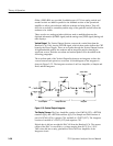
In order to protect the analog input and reference voltage inputs of the ADC, the
input amplifier section is required to clamp the incoming LOGVID signal
between ±2.3 V. The input amplifier clamps in the negative direction at --0.7 V,
due to diode CR2. The diode in the output of U2 prevents the operational
amplifier from going below ground, which in turn limits the voltage at the
emitter of Q3 to about --0.7 V. Clamping in the positive direction occurs when
the operational amplifier reaches its positive rail, the signal is attenuated by the
resistive divider, R29 and R31, and then shifted down by two diode drops. This
prevents the signal from exceeding the positive input voltage specification of U1.
There are also three reference supply circuits on this section. The main reference
supply is +VR, at +5 V. It is generated using a TL431 precision Zener reference,
buffered through U5, one half of an MC34002 operational amplifier and then
driven by Q1, a BCX68 npn transistor. Power dissipation on the output transistor
for +VR requires an SOT--89 style package. A negative reference supply is
generated from +VR. This negative reference is --VR, at --5 V. The other half of
U5 is used to buffer this supply. --VR is driven by Q7, a BT3906 pnp transistor.
The final reference supply is the +2 V reference for the ADC. This supply is also
generated from the +VR supply. It is buffered by another MC34002, U4. The
output transistor for this reference supply is Q2, a BT3904 npn transistor.
Vertical Data Processor and NVRAM. The Vertical Data Processor and NVRAM
section performs all of the waveform data processing, storing, and nonvolatile
RAM (NVRAM) arbitration. It consists of an XC3042 LCA (U15), a single
XC1736 serial configuration PROM (U14), two TC55257 32K by 8 SRAMs
(U13 and U30), and two DS1210 Nonvolatile Controller ICs (U6 and U28).
At power up U15, the Vertical LCA, will wait until the BDRST_L signal
becomes high and then begin configuring itself from the contents of U14, the
serial configuration PROM.
During normal operation U15 receives data, at the falling edge of BCLK,
directly from the A/D Converter via the VAD<7..0> bus. This data is manipu-
lated inside U15, depending on the acquisition mode, and then written to the
NVRAM. If the acquisition mode is Max Peak, the incoming data is compared
against the data already stored in the Max Accumulator (a register internal to
U15). If the incoming data is greater than the Max Accumulator then the
incoming data becomes the new value stored in the Max Accumulator.


