Theory of Operation
2715 Spectrum Analyzer Service Manual
3-65
Reading from a module begins with the module requesting service through its
active low request signal (FPREQ-- for the front panel, ...). This signal goes into
a priority encoder (U780) on the Power Supply Secondaries, then pulls the
Microprocessor board Interrupt Handler, IRQ1, high. The outputs of the priority
encoder are then used to acknowledge the request for service that activates the
output buffers on the module requesting service. At the same time, the outputs of
the priority encoder, ADI0 through ADI2, are fed into the I/O Subsystem status
register, U595. This status register is then read, due to the interrupt, and the
address of the module requesting service is determined from the ADI0 through
ADI2 lines. Now the process of reading in the data from the module requesting
service can begin.
The lowest bit of the I/O Subsystem status register contains the data from the
module to be read. After each CLKI-- signal, the status register is read and the
data is linked together in a series until all data has been received. The CLKI--
signal is generated the same way as the CLKO-- signal described earlier.
The memory on the Microprocessor board consists of two sections, 128 kilobytes
(16 × 8 kilobytes) of Random Access Memory (RAM), and up to 524 kilobytes
(64 × 8 kilobytes) of Read Only Memory (ROM). The RAM is used for CPU
processing and data space, while the ROM contains all of the system firmware.
Access to the RAM, for either reading or writing, consists of sending out the
address for the byte to be accessed. This address is decoded by U515, and the
appropriate enable line pulled low to select the memory device that is to be
accessed.
Access to the ROM (read only) is performed in the same way as the RAM.
Jumpers (and wires for a more permanent method) are provided on the Micropro-
cessor board for selecting the size of EPROM and RAM memory chips used.
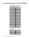
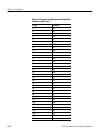
Table 3 --16 shows the configuration of jumpers/wires for various size memory
ICs.
Table 3- 16: Configuration of Jumpers/Wires for
Various Memory IC Sizes
Memory Size Jumpers/Wires to Install
27256 W525A W518B
27512 W525A W518A W522
27010 W525A W518A
27020 W525B W518A
43256 W526A
4364 W526B
Memory


