


Theory of Operation
2715 Spectrum Analyzer Service Manual
3-31
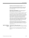
In phase locked spans, its output is used to fine tune the VCO frequency. In
either case its output passes through U852, which has an output range of 0 to
+5 V. U845 sums that with an offset and provides gain so that the output of U845
ranges from --5 V to +5 V. This signal is called VCFC (L/FM) and is routed to
the appropriate destination by U757A and U757D.
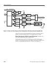
Main Coil DAC U950A output passes through U952 and U940. U940 provides
gain such that the output of U845 ranges from --5 V to +5 V, and the result is
summed with the other components of the main coil current. Its function is
coarse tuning of the 1st LO center frequency, in steps of approximately 400 kHz.
U950B is the PLL DAC . Its function is coarse tuning of the VCO frequency. Its
output is converted to the --5 V to +5 V range by U954 and U941 before being
summed with the other components of the VCO tune voltage.
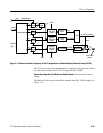
Unlike the other DACs, U850B’s reference input is supplied with the analog
sweep waveform SWP (from the Sweep board through U565) and serves as a
microprocessor controlled gain control to determine span/div. Its output passes
through U854 to a decade attenuator composed of U831 and associated
components. The output of the decade attenuator is then routed to the desired
destination by switches U830A, U830B, and U757B. In wide spans, this signal
sweeps the 1st LO main coil. In moderate spans, it sweeps the 1st LO FM coil.
In phase locked spans, it is used to sweep the VCO frequency.
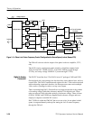
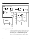
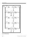
This circuitry links the phase lock hardware with the microprocessor. The link is
bidirectional. Commands and DAC setting data are sent to the PLCFC module,
and lock status information is sent back to the microprocessor. In addition, there
is provision to loop input data back to the microprocessor to verify integrity of
the interface circuitry.
The path into the PLCFC module is through a 24 bit shift register composed of
U361, U460, and U560. Serial data on the DATAO line is shifted into the
register by the clock signal CLKO. When all 24 bits have been shifted in,
CFLATCH-- is used to latch data simultaneously from all shift register stages to
parallel output registers. The resulting 24 bit parallel word is used to control
switches, set DACs, and do a number of other things on the module. A listing of
the 24 lines and their functions appears later in Table 3--22 on page 3--71.
CFCLATCH-- also triggers U372 causing a delayed pulse on the WR-- line,
latching data into internal registers of the DACs.
U370 is an 8 bit shift register used for transferring data from the module back to
the microprocessor. Serial data is shifted out on the DATAI line by the clock
CLKI--, which is gated into the clock input of the register by U270C as
controlled by C FCACK--. Data may be serially loaded into this register through
the EXAM line coming from the tail end of the 24 bit input register. In this
situation the data is clocked into the register by a derivative of CLKO, which is
gated by LOADEXM through U270D.
Digital Interface