Theory of Operation
2715 Spectrum Analyzer Service Manual
3-69
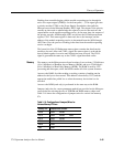
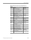
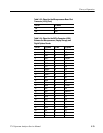
Table 3- 19: Microprocessor Interface Connector (J550) Signal Names and
Definitions
Signal Name Description Source Module
BUSDIS Bus Disable (TTL): Disables microprocessor
address bus and control signals
Display Storage
Digital Options
ALE Address Latch Enable (TTL): Signal used to latch
the address lines into the address registers.
Microprocessor
BCLK Buffered Clock (TTL): Microprocessor crystal
oscillator divided by six, 92.4576 M Hz
Microprocessor
BRD-- Buffered Read (TTL): Microprocessor signal
signifying a read cycle
Microprocessor
BWR-- Buffered Write (TTL): Microprocessor si gnal
signifying a write cycle
Microprocessor
BIO/M Buffered I/O or Memory (TTL): Microprocessor
signal used to determine if the read or write cycle
is for an I/O device or memory
Microprocessor
BRST-- Buffered Reset (TTL): Microprocessor reset line Microprocessor
BWAIT-- Buffered Wait (TTL): Line to Microprocessor used
to insert wait states
Display Storage
Digital Options
BD0 through
BD7
Buffered Data (TTL): Mic roprocessor bidirectional
data lines
Microprocessor, Display
Storage, and Digital Option
BA0 through
BA19
Buffered Address (TTL): Microprocessor address
lines
Microprocessor
BMT-- Boot Memory Test (TTL): Maps an optional ROM
on the GPIB or R S-232 board to high address
space for diagnostics
Digital Options
IR4 Interrupt 4 (TTL): Interrupt line to the interrupt
handler on the Microprocessor board
Digital Options
IR5 Interrupt 5 (TTL): Interrupt line to the interrupt
handler on the Microprocessor board
Digital Options
VPROG Voltage Program: Programming voltage for
EPROMs on the Microprocessor board
External Programmer
ROMVCC ROM Power Supply: Power Supply that is
selectable for either programming voltage levels
or operating voltage levels
Microprocessor
External Programmer
+5 V +5 V Supply: +5 V supply f rom Microprocessor
(power supply module) t o modules connected to
J550
Power Supply


