


Theory of Operation
3-64
2715 Spectrum Analyzer Service Manual
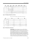
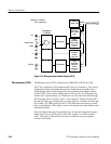
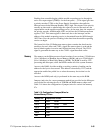
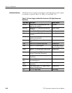
Table 3- 15: Interrupt Controller Input
Connections (Cont.)
Interrupt Number System Connection
IR5 Digital Options Board
IR6 Digital Options Board
IR7 Programmable Interval Timer 1
See the NEC PD71059 (or Intel 82C59) data sheets for more detailed informa-
tion on the operation and programming of the Interrupt Controller.
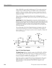
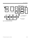
The I/O Subsystem performs the serial communication between the CPU and
other modules in the instrument, controls the Interval Timers, and triggers single
sweeps.
The signal SSTRIG (pin 5 of U495) is used to trigger the single sweep mode of
the instrument. This signal is selected by writing a one to the second LSB of the
I/O Subsystem Control Register.
The I/O Subsystem Control Register is also used to control some parts of the
Interval Timer (U580). The signal, GATE_0 (pin 6 of U495), is used to enable
Timer 0 of the Interval Timer depending on how the counter is set up.
The signal AUDEN is used to enable Timer 2 of the Interval Timer. This timer’s
output is a square wave, UPAUD, which is used by the Log board to generate the
audio feedback tones that are heard on the speaker.
The serial bus is used by the CPU to communicate with several of the modules
in the instrument. The serial bus is based on either a three wire or seven wire
system. The three wire system is used for modules that only listen (are written
to), while the seven wire system is used for modules that must talk and listen.
Writing to a module begins by latching one bit of data into the Q0 register of
U495 and generating a strobe on the XCLKO-- signal. The strobe is generated by
writing the correct address to U585. The XCLKO-- output (pin 16 of U585) then
goes low for two clock cycles of the CPU (the length of the WR-- pulse). This
strobe is used as a shifting clock to load a single bit into a shift register on all
modules (connected to the DATAO signal).
After all of the data for the intended module has been sent, a 4 bit address,
ADO0 through ADO3, is latched into U495 registers Q4 through Q7. This 4 bit
address is decoded by U590 on the Power Supply Secondaries and becomes the
latch pulse for the intended module latches. The latch pulse is generated by the
LOAD signal (pin 13 of U585) and is two CPU clock cycles long. All modules
must have a pull up resistor on the incoming latch signal in order to guarantee
correct logic levels.
I/O Subsystem Interface