


Theory of Operation
2715 Spectrum Analyzer Service Manual
3-47
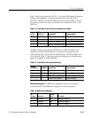
Marker Position Registers. There are two Marker Position Registers. One register
for Marker 1 and a second register for Marker 2. Marker Position Register 1 uses
I/O port locations 0x0FC00 through 0x0FDFF. Marker Position Register 2 uses
I/O port locations 0x0FE00 through 0x0FFFF. Each port location corresponds to
a horizontal position on the screen. By writing any data to one of the I/O ports
inside the above range, the corresponding marker will be placed at the horizontal
position, on the CRT, represented by the lower nine bits of the port address.
For example, writing 0x55 to I/O address 0x0FCE3 will place Marker 1 at
horizontal screen position 0x0E3 (227), while writing 0xA1 to I/O address
0x0FFF9 will place Marker 2 at horizontal screen position 0x1F9 (505).
The Display Storage board is best described by breaking it up into several
sections. These sections include Address Buffering and Decoding, the Control
Registers, the Horizontal Input and Tracking A/D, the Vertical Input, the Vertical
Data Processor and NVRAM, the Readouts and Waveform Drawing, the
Horizontal Output, the Vertical Output, and the Miscellaneous Decoupling. The
following sections will describe each one of these in detail.
Address Buffering and Decoding. The Address Buffering and Decoding section
consists of a 74HCT245 bidirectional bus transceiver (U22), and a GAL20V8
PA L (U29). The purpose of this section is to decode the incoming address lines
into the various enable signals required by the Display Storage board, buffer the
data lines from the CPU Board, and buffer the BCLK signal for distribution
around the board.
U22, the bus transceiver, is used to allow data on or off the Display Storage
board. This bus transceiver can only be enabled after the RAM arbitrator grants
access to a request from the Microprocessor.
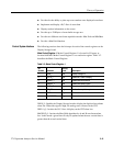
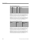
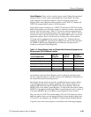
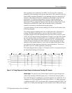
The PAL, U29, decodes the address lines BA19 through BA9, to generate the
request signal UPR EQ, and the enable signals PORTVEC, MKR1_LT, and
MKR2_LT. In addition the signals RDEN and WREN are generated on read or
writes to or from the board. The memory map (Table 3--11) shows which signals
are generated from which address ranges. A description of each signal from U29
is given below.
UPREQ. This signal becomes active (high) any time the board is accessed by the
CPU. The UPREQ signal is fed into the RAM arbitrator to request access to the
board.
PORTVEC. This signal becomes active (high) at any access to the Control
registers (I/O port addresses 0xFA00 through 0xFBFF). This signal also causes
the UPREQ signal to become active.
MKR1_LT. This signal becomes active (high) at any access to the Marker 1 port
addresses (I/O port addresses 0xFC00 through 0xFDFF). This signal also causes
the UPREQ signal to become active.
Circuit Description