Theory of Operation
2715 Spectrum Analyzer Service Manual
3-59
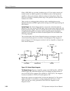
The Error Amplifier compares the current state of the Integrator Circuity output
and the current input voltage from the DAC and generates an error voltage. This
error voltage is then fed into a high current buffer made up of Q4, Q5, and CR7.
CR7 and R179 are used to insure that transistor Q4 is properly biased. The high
current buffer is required to ensure that the capacitor in the Sample and Hold
section is charged quickly. The Sample and Hold circuit basically samples the
error voltage by closing the analog switch, U34, for 400 ns, charging capacitor
C94. When the switch opens the value of the error voltage should be across the
capacitor. The operational amplifier U57 then buffers and amplifies the error
voltage such that when it is applied to the Integrator sexton ramp the correct
slope is produced. The potentiometer, R181, Vector Length, is used to adjust the
slope of the output ramp to match the waveform data drawing rate. The input of
the Integrator section consists of two resistors with a capacitor to ground
between them. This R C network, along with the resistor in series with the
integrating capacitor, C93, form a network that prevents an early step when
integrating over a long distance. The step is caused by the rapid change in error
voltage coupling straight through the integrating capacitor. The resistors R112
and R183 along with capacitor C93 and operational amplifier U57 form the
Integration Section of the Integrator. The output of the Integrator is then fed
through a DC641 analog switch and into the output buffer, U35, of the Vertical
Output Section. Finally a potentiometer, R174, Vector Offset, is provided to
compensate for the injection charge of the DC641 into the hold capacitor, C94.
The signal for drawing the Readouts is taken directly off U4, the DAC current to
voltage buffer, and fed through an analog switch into the output buffer. The gain
variations between the waveform and readout is accomplished by slightly
increasing the gain of the Integrator, such that the Readouts will always remain
inside the graticule. In order to ensure that the Readouts will always appear
centered inside the graticule, the waveform is forced slightly lower by adjusting
the Vertical Offset to +40 mV. Then when the waveform display is centered on
the screen using the Vertical Output Offset potentiometer everything aligns
correctly.
The final buffer in the Vertical Output Section provides both gain and offset
adjustments, Vertical Output Gain (VOG), R42, and Vertical Output Offset
(VOO), R63. The two analog switches which drive the DSVER signal are used
to switch between the LOGVID signal, for real time analog display, and the
VERT signal for digitized display (readouts).
Miscellaneous Decoupling. Contained on the Miscellaneous Decoupling page of
the schematics are all of the decoupling capacitors. There is one 0.1 F capacitor
for each digital integrated circuit on the board. Also shown on this page are
several 221 Ω resistors. These resistors are required to restore the power
dissipation to a minimum level to ensure that the power supply can maintain its
supply voltages well centered.
Power Up Reset. The power up reset circuit is included to ensure that a valid reset
signal is generated when the instrument is turned on.


