


Theory of Operation
2715 Spectrum Analyzer Service Manual
3-49
Control Registers. There are five control registers on the Display Storage board
which are used to set the various operating modes for the board. All of the
control registers are read/write registers, with the exception of the Scroll
Register. The Control R egister section consists several 74HCT273 latches and
74HCT541 tristate buffers, and two 74F138 decoders.
Each control register is made up of a 74HCT273 latch and a 74HCT541 tristate
buffer. During power up each control register is cleared to all zeros, allowing the
board to start at a known state. Table 3--12 gives the reference designators for
both the latch and tristate buf fer used for each control register. The two 74F138
decoders are used to decode the BA2, BA1, and BA0 address lines to select the
appropriate register. There is one decoder for writing to the control registers,
U16, and one for reading from the control registers, U17. Both decoders are
enabled by the PORTVEC signal from the Address Decoder Section and either
the WREN or RDEN signal (depending on whether the microprocessor is
reading or writing the Control Registers).
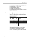
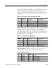
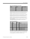
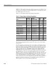
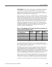
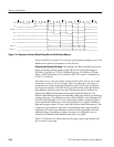
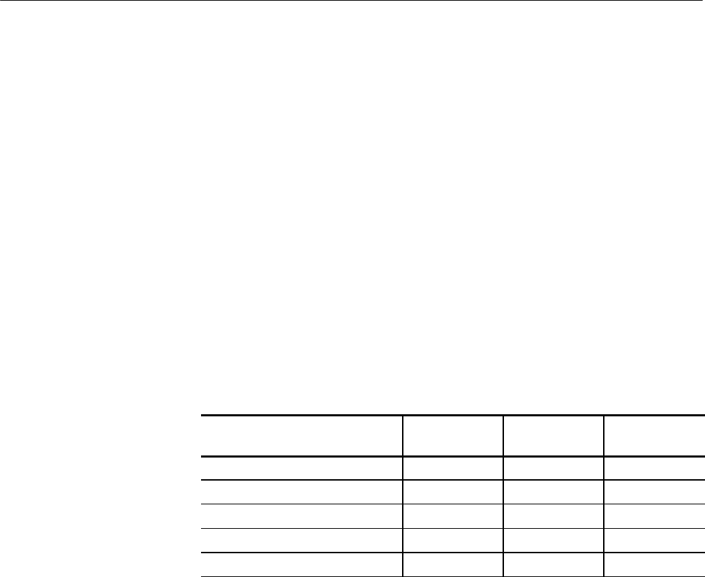
Table 3- 12: Control Register Latch and Tristate Buffer Reference Designators and
Microprocessor I/O Port Address Locat ion
Control Register Name
Latch Ref.
Designator
T ristate Ref.
Designator
Port Read/
Write Address
Mode Control Register 1 U18 U20 0x0FA00
Marker Save Register U23 U26 0x0FA01
Display Control Register U21 U25 0x0FA02
Scroll Register U19 N/A 0x0FA03
Mode Control Register 2 U24 U27 0x0FA04
As mentioned earlier the Scroll Register can’t be read by the microprocessor.
This is to allow the ability to read the contents of the Maximum Accumulator in
the Vertical Waveform Processing Section.
The Display Storage board also provides an additional control register, Mode
Control Register 2 to protect against accidental writes. This protection is an
enable bit (MCREG2) located in the MSB of the Scroll Register. While the
MCREG2 bit is low, Mode Control Register 2 is held in the cleared state. When
MCREG2 is brought (and held) high, Mode Control Register 2 can be written. If
at any time MCREG2 goes low, Mode Control Register 2 will be cleared.
There are also two 74HCT541 tristate buffers (U32 and U33) which are used to
buffer the address lines on to the internal (Display Storage board’s) address bus.
U32 and U33 are enabled by the UPGRNT_L signal from the RAM Arbitrator.
A typical write to the control registers is described in the following paragraph.