


Theory of Operation
3-76
2715 Spectrum Analyzer Service Manual
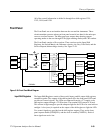
The battery backup circuits consist of a 2.8 V lithium battery (BT1), and two
DS1210 (U16 and U17) power monitor chips. U17 supplies backup power for
the RAM (U8), likewise U16 supplies the real time clock (U23). The DS1210
chips supply power from the power supply while its voltage is above 4.75 V and
switches to the 3 V battery backup supply when the power supply voltage falls
below 4.75 V. The chip select outputs of the DS1210 chips go high when
switched to battery backup power. This guarantees that the SRAM and RTC will
not be written to during the power down sequence.
The RS--232 ports are implemented by a Z85C30 SCC chip (U22) and an
LT1130A transceiver chip (U9). To read or write to one of the internal registers
of the SCC one must first write to WR0. The data written to WR0 will contain,
in the lower six bits (bits D0 through D5), a pointer to the desired register. The
next read or write cycle then either reads or writes the register that is pointed to
by WR0. At the end of the second read or write cycle the pointer value in WR0
is reset to zero (next write defaults to WR0). Wait states are inserted during
writes due to the timing requirements of the TTY_WR_L signal and the access
recovery time requirements of the Z85C30.
The GPIB section is composed of the 9914A, GPIB Controller IC (U18), a
75160 GPIB octal bus transceiver (U19), and a 75162 GPIB eight channel
transceiver (U20). In addition there is circuitry included to drive two LEDs.
These two LEDs display the status of the Not Ready For Data (NRFD) and Not
Data Accepted (NDAC) handshaking lines.
The 9914A, as well as the 75160 and 75162, meet the IEEE-- 488.1 standards.
Access to the 9914A is through the microprocessor address and data buses,
where the lower three bits of the address bus (A0 through A2) determine which
of the thirteen internal registers are to be accessed (6 readable, and 7 writeable).
For GPIB programming information, refer to the 2714 and 2715 Programmer
Manual.
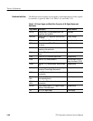
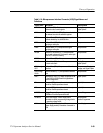
The entire address space of 0x0e800 to 0x0efff is occupied by this read only
register. In addition to three interrupt status lines, this register also contains other
miscellaneous status. The GPIB_DIR_L status bit indicates the direction of
GPIB data flow. The DONE_PG bit is an output from the Xilinx part which goes
high when self programming is complete. The software must check this bit
before attempting to write to any of the registers on the Xilinx part. If the
DONE_PG does not go high within 500 ms of power up the software should
attempt to reset the system by forcing the BRST_L line low. If DONE_PG still
does not go high within 100 ms, a diagnostic message should be displayed
indicating a hardware failure.
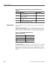
Battery Backup Circuit
RS- 232 Serial Port
GPIB Interface Port
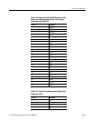
Input Vector Register