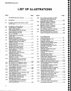
LIST
OF
ILLUSTRATIONS
(Conr.)
Page
Flgure
I
o
o
a
o
I
I
o
o
a
I
a
t
o
I
I
o
t
o
o
I
t
o
a
o
o
a
o
I
I
a
o
o
o
I
o
I
o
a
o
o
o
o
I
494A/494AP
Servtce
Vot.
1
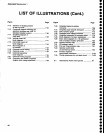
Figure
5-21 PreseleetorDriver
adjustment
setup.
.........
............5_22
5-22 Preselector
Driver
test
point
and
adjustment
locations
...........
S_Zg
5-23 Test
equipment
setup
for
band
leveling
adjustment.
,.................-
S-24
5-24
Band
leveling
adjustment
and
gain
diode locations.
...-.....,,,....5-24
5-25 Test
equipment
s€tup
for
adjusting
the
phase
Lock
assembly.
...........................
5_26
5-26
Phase
Lock
assembly
adjustment
and
test
point
locations.
.............,.................
S_27
5-27
Option
42
adjustment
test
equipment
setup.
.........
.............
S_g0
6-1
Surface-mounted
components
lead
configuration.
....................
6_1
6
6--? Diode
potarity
markings.
..........
6-18
9-9
Multipin
(harmonica)
connectors.
.................
6_1g
9-1
Servicing
the
vR
assembty.
......
6_19
9-9
Topdeckassembties.
.............................,-...6-20
6-6 RF
deck assemblies.
................
6_2.1
6-7 Removing
the 1st
LO
Interface
board.
.....
6-25
9-9
Fan
assembty
mounting.
..........
6-26
6-9
110
MHz
lF return
loss
adiustment
setup.
.........
............6-2T
6-10 110
MHz
tF
test
points
and
adjustments.
..........
............
6-2g
6-11
2072MHz
Converter
bias
_
adjustments.
..........
6_2g
6-12
829
MHz
LO
test
points
and
connectors.
...........
............
6-29
6-13
829
MHz
amptifier
test
iack
and
jumper.
....
6_30
6-14
829
MHz
filter
test
equipment
setup.
.........
.............
6-gi
6-15
829
MHz
Converter
filter
tune
tabs.
.............
6-32
6-16
Correct
response
for
929
MHz
first
and
second
resonators.
....
6-92
6-17 Correct
response
for
829
MHz
third
and
fourth
resonators.
.........................
6_9g
6-18
2182MHz
2nd
LO
frequency
-
accuracy
test
setup.
........
.........
6_94
6-19
2182MHz
phase
Locked
2nd
LO
adjustment
setup.
.........
............
6_96
6-20
16-20
MHz
phase
Lock
circuit
test
point
and
component
locations.
................,..
6_32
6-21
2182MHz
2nd
LO
adjustment
6-22
Coaxial
test
probe
Page
construction
details.
..................
6-gg
6-23
2182MHz
2nd LO
Phase
Lock
adjustment
setup.
........
..............
6_39
6-24
Tune
and
Sweep Range
adjustments
............641
6-25
3rd
Converter
test
points
and
adjustments.
..........
............
6_43
First
Converter setup
for adjustment.
..........
6-45
1st
LO Driver
board adjustment
and
test
point
locations.
...............................
646
Baseline
leveling
test
setup,
.....647
Typical
baseline
leveling
response.
.............,
649
Baseline
leveling
adjument
and
test
point
locations.
...............................
649
Typical
baseline
compensation
response.
...........
6_49
6€2
A15
through A12 in
microcomputer
test mode.
.......
6-52
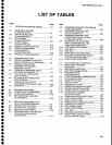
6-33 Four
main
bloack select
outputs
of address
decoder
U2045.
......
6_59
6-34
RAM
select output
in
relation
to
O'XXX.
...................
6-53
6-35
RAM setect
output
in
relation
toTffi.
...................6-5g
6-36
-UOand
S1050 setect
tines
in
relation
to
oxxx.
...................
6-53
6-37
Chip
selects
Y0, Y1,
yS,
and
Y7 in retation
toT/O-.
...........
6-54
6-38
Chip
selects
Y2, Y4,
and
y6
in
retation
td:IIO.
..
6-54
6-39
Instrument
bus check.
..............
6-55
7-1
Cross
section
of
a
four-cavity
filter. ..........
..........
7-g
7-2
Equivalent
circuit of
the
four-cavity
filter.
..................
7-g
7-3
Simplified
diplexer
diagram.
.....
7-19
7-4
Equivalent ac
circuit
of
an
829
MHz
amplifier.
..................................
7-1
4
7-S
Equivalent
dc
circuit
of
an
829 MHz
amplifier.
..........................,.......
7-'t
4
7-6
Block
diagrarn of
the
phase
lock loop
in
the
829
MHz
2nd
Converter.
....................7-16
7-7
Bridged'T"attenuator
equivalent
circuit.
.....................
7-lg
7-8
Block
diagram
of
a
three
stage
log amplifier.
....................
7-29
7-g
Log
amplifier
gain
curve
showing
break
points
.................
7-90
7-14
Curve
showing
end-of-range
for a log amplifier.
....................
7-gO
7-11
Simplified
detector
circuit.
........,2-gz
6-26
6-27
6-28
6-29
6-30
6-31
xl


