


I
o
I
o
a
o
o
o
o
o
o
,
o
o
o
I
o
o
o
I
t
o
e
o
o
O
I
o
a
a
I
I
o
a
I
I
I
o
o
o
a
I
a
o
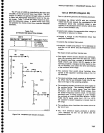
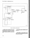
lF
Ofiset
The
-10
V
reference,
from
the oscillator
driver,
fur_
nishes
the
precise
reference
vo,tage
for
the
lF
offset
circuit.
Since
the
offset
voltage
is
pioportionat
to
the lF
mings
2.072
GHz,
no
ottset
id
requireo
for
the
+2.072
GHz
tF.
FET
02094
adds
th€
*829
MHz
net-
work
into
the circuit
and
e2036
adds
the
_829
MHz
nehi/ork.
Data
bits DB6
and
DB7
through
two
compara-
tors in
U5022,
control
the
two
FET
swirches
e203i
and
02036.
One,
but
not
both,
transistorb
are
switched
on
to
provide
the offset
voltage
to
the
inverting
input
of
U2045.
An
output
voltage
of
_-9
V from
the
amplifier
corresponds
to
-2901
MHz
or
(_0esnHzy_zot2MHzl.
_
The
signat
on
the
FINE
TUNE
VOLTS
tine,
from
the
Center
Frequency
Control
board,
which
is
used
to
tune
the
2nd
Locat
Oscillator,
is
appli€d
to
the
input
of
U2O47.
Since
it
is
apptied
here,-ii
is
independent
of
the
voltage
tripling
action
in
the
voltage processor
circuit.
T!:.lulilg
voltage
is atso
applied
to
the
input
networks
of
U2045
through
R9044,
O2Og4,
and
R1037,
02096.
By
varying
the
magnitude
of
signal
in
the
inverting
path
compared
to
the
direct
path,
the
proper
magnitudl
and
polarity
of
fine
tune offset
for
each
lF
is
provided.
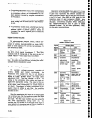
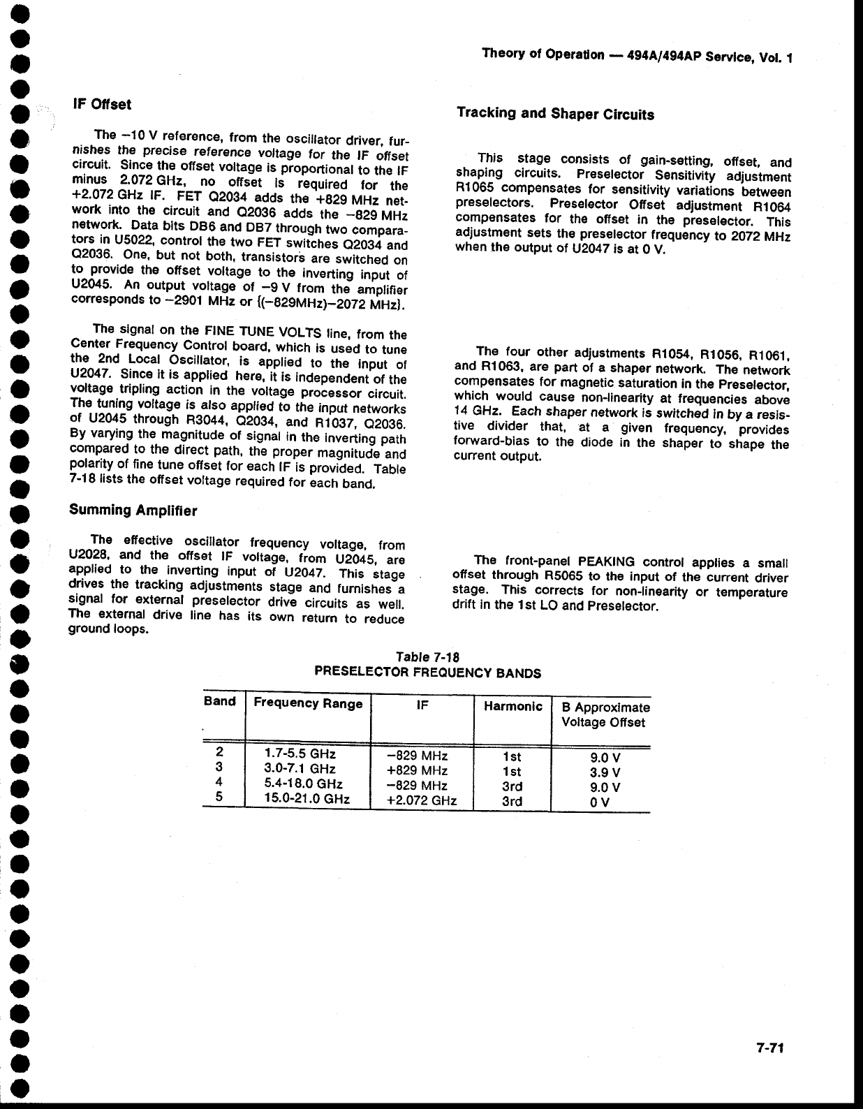
Table
7-18
lists
the offset
voltage
required
for
Lach
band.
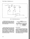
Summing
Amplifier
The
effective
oscillator
frequency
voltage,
from
U2028,
and
the offset
tF
voltage,
tiom
U2b+5,
are
appfied
to
the inverting
input
of
U2C/T.
This
stage
drives
the
tracking
adjustments
stage
and
furnishes
a
signal
for
external preselector
drivl
circuits
as
well.
The
external
drive
line
has
its
own
r€turn
to reduce
ground
loops.
Theory
of
Opera0on
-
4g4\l4g4Ap
Servlce,
Vot.
I
Tracking
and
Shaper
Circuits
This
stage
consists
of
gain-setting,
offset,
and
shaping
circuits.
preselector
Sensitiviiy
adjustment
R1065
compensates
for
sensitivity
variations
betwe€n
preselectors.
Preselector
Offset adjustment
R10O4
compensates
for
the offsst
in
the
presel€ctor.
This
adjustment
sets
th€
preselector
frequency
to 2OTZMHz
when
the
output
ot LJaO4T
is
at
O V.
The
four
oth€r
adiustments
R1054,
R1056,
R1061,
and
Rl
063, are
part
of
a shaper
network.
The
network
compensates
for
magnetic
saturation
in
the
pr€selEctor,
which
would
cause
non-linearity
at frequencies
above
.1.4
GHz.
Each shaper
network
is
switched
in
by a resis-
tive
divider
that,
at
a
given
frequency,
provides
forward-bias
to
the
diode in
the shap€r
to shape
tne
current
output.
The
front-panel
pEAKING
control
applies
a small
offset
through
R5065
to the input
of
the
current
driver
stage.
This
corrects
for
nonjinearity
or
temperature
drift
in
the l st
LO
and
preselector.
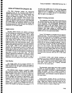
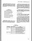
Tabte
T-18
PRESELECTOR
FREOUENCY
BANDS
Band
Frequency
Range
IF
Harmonlc
B Approximate
Voltage
Offset
2
3
4
5
1.7-5.5
GHz
3.0-7.1
GHz
5.4-18.0
GHz
15.0-21.0
GHz
-829
MHz
+829
MHz
-829
MHz
+2.472
GHz
1st
1st
3rd
3rd
9.0
v
3.9 V
9.0
v
0v
7-71