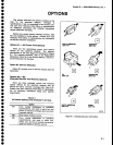
Theory
of
Operaton
-
494A/494Ap
Servtce,
Vot.
1
u$36.
PrN
2
u603A
PIN
3
u6036,
P|l{
7
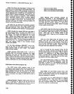
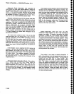
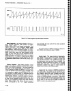
Figure
7-34,
Primary
.egutator
Input
and output waveforms.
a
o
o
O
o
o
o
a
o
o
o
o
o
o
o
a
o
o
o
o
o
o
o
o
o
o
o
O
o
o
a
o
o
o
o
o
O
o
o
o
o
o
a
o
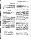
Ramp
Generator.
The
ramp
generator
circuit
is
a
gated
sawtooth
generator
that
consists
of
T6044.
Q5023, Q6034,
Q5032,
and
related
components.
The
negative
excursion
of
the rectangular
shaped
signal
from
U6059 is coupled
across
T6044
to force
e6094
into conduction.
This
foruvard-biases
e5032.
lts
coll€c-
tor moves
toward +17
V
to
charge
Csogg
to this
value.
06034 loses
drive
(since
the
pulse
coupled
across
T6044
has
died away)
and
the
two
transistors
cut
off.
05023 acts as
a constant-cunent
drain
to linearly
discharge
C5038.
This
signal
is coupled
across
divider
R5036/R6032,
then apptied
through
C6Og9
to
the
input
of comparator
U6036,
which
is
part
of
the
primary
regu-
lator.
Prlmary
Regulator.
The
primary
regulator
circuit
consists
of comparator
U6036
and
U6046,
photocoupler
U6043,
and
related
components.
The
circuit
varies
the
duty
cycle
of
the
driving
signal
for
the inverter.
The
+17
y
is
divided
by R6038
and
R6097
to approximatety
+4.8V
and apptied
to
the inverting
input
of
U6036.
Thi
+5 V reference
is apptied
through R6022
to the
non-
inverting input
of
u6036,
where
it is
combined
with
the
ramp signal
from
the
ramp
generator
stage.
The
non-
inverting
input
receives
a
sawtooth
signal
of approxi-
mately
500 mV
peak-to-peak
superimposed
on
a +S
V
dc level.
This
is compared
with
the +4.9
V
on
the other
input, so
the
comparator
switches
with
each
sawtooth
cycle. Note
in
Figure
7-34
that
as
the
level at
pin
g
(which
corresponds
to the +I7
V
supply
variations)
7-104
rises
and falls,
the duty
cyele
of
th€ output waveform
varies accordingly.
The output
signal of
U6036
is applied
to
optical
iso-
lator
u6043, which
drives the input
of
u6069,
lnverter
Loglc. This stage consists of steering flip-
flop
U6063B
and dual
quad
input
NAND
gate
U6069.
The flip-flop
is connected so it
toggl€s
to enable first
one
gate
then the
other.
The sguare-wavg
output
from
the
multivibrator
drives
the
clock
input
of U60638. The
signal also
enables
each
gate
to
ready it for
the other
signals
that
arrive later.
The
output
state
of
U60638
determines whether
the upper
or lower section
of
U6069
will
be
ready for
the
enabling signal.
Assume
that the Q
output
of U60638
is
holding
pin
2
of
U6069 high. This means
that the
complement out-
put
of
the
latch is holding
the
opposite
side of the
gated
pair
disabled.
When
the
output of
U6043
moves high,
U6043
controls
the duty
cycle of
the
inverter, the upper
section
of
U6069
produces
a
low
state.
This
causes
current
to flow
through
half
the
primary
and Q6078
only.
On the opposite cycle of
the
multivibrator
signal, the
latch is
reset, so
the
lower half of
U6069
is enabled
and
Q6077 is now in
the
conduction
path.


