


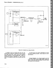

Theory
of
Operaton
-
4g4Ll4g4Ap
Service,
Vol.
1
CR2068.
CR1065
provides
a
clamp
to
prevent
a
control
line
voltage
less
than
5
V.
Capacitor
C1070
sets
the
low
end
of
the
control
voltage
to about
6 V.
Range
of
the control
voltage,
over
the 20A-Z2O
MHz
VCO
,ing",
is
about
*6 V
to +11
V.
The off/on
status
of
the VCO
is
controiled
by
U4074
which is
activated
by D3
from
the
data
bus.
The value
is latched
in
U4074
and
its output
turns
e2076
off
or
on.
The
output
also
controls
the sensitivity
of
divider
U5015.
During
the
period
when
the VCO
is
6tr
anO
there
is
no
input
signal,
the
divider
sensitivity
is lowered
so
stray
signals
wlll
not
activate
the
divider.
This
is
done
by
turning
05027 on
and
puiling
input
pin
6
of
U501S
tow.
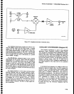
The
100MHz
signal
from
the
grd
Conv€rter
is
applied
through
a
resistive power
splitter
to
divider
U2017 and
to buffer amptifier
el015.
The
1 MHz
output
from
the
divider,
U2A1T.
is further
divided
by
5 within
the synthesizer
lC,
to
b€come
the 200
kHz
reference
frequency
for
the synthesizer.
The
amplifier
e1015
has
negative
fEedback
for
gain
stabilization.
lts
output
sig-
nal
is
applied
to
the counter
board.
The
10-80
MHz
signal
from
the harmonic
mixer
is
passed
through
a 7-pole
low-pass
filter
with
g0
MHz
cutofi.
The
signal
is
then
amptified
by
U4021
with a
broad
band
gain
of about
24
dB.
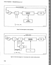
COUNTER
BOARD
(Diagram
38)
The
Counter
board
circuits
and
function
are:
1) The
address
decoder
which
receives
and
decod€s
th6
talk
and
listen commands
for
the
microcomput€r.
2) The
service
request
circuits
that
sense
an
impending
loss
of
lst
LO
phase
lock
and
sends
a service
request
to
the
microcomputer.
lt
then
cancels
the
request
when
directed
by
the
microcomputer.
3)
The
data
bufiers
transmit
data
to
and
from
the
microcomputer.
4) The
input amplifiers
and
multiplexer
amplify
input
signals
up
to
TTL levels
and
then
select
which
of
the inpui
signals
is
to b€ counted.
5)
The
+2n
counter
divideJ
the
selected
input signal
by some
power
of
2 as
determined
by
the
microcomputer.
6)
The
21-bit
counter
counts
at a
100MHz
rate
for
a
given
number
of
cycles
of
the
selected input
signal.
Address
Decoder
The
addresses
from
the
microcomputer
are
decoded
by address
decoder
U2040.
The
counter
cir_
cuits
hav€
both a
talk address,
where
the counter-buffer
circuits
are
instructed
to
talk on
the
data
bus, and
a
fisten addr€ss,
where
UgA24
is
directed
to
receive
data
from
the
data
bus.
The
talk address
is
Fg;
the
listen
address
is 73.
Service Request
Circuits
The
service
request circuits
consist
of
multiplexer
U3040, latch
U30488, and associated
circuitry.
This
cir-
cuitry
alerts
the microcomputer
in
the
event
that
the
lst
LO
has
drifted too far.
The
UP
and
DOWN
signals
from
the
window
comparator
(located
on
the Error
Amplifier
board) drive NOR
gate
U3010C. Both
signals
are also
sent
to
U3034,
where
their status
can
be read
by the
microcomputer.
When one
of
these signals
is
high, it
indicates
that the Error Amplifier
is
approaching
its
operating
limits and
the microcomputer
should
actjust
the
lst
LO frequency so
the
Error
Amplifier returns
to
th€ c€nter of its range.
A high
at
either input
of
u3010c
produces
a negative
transltion that ls
inverted
by
U3046C.
C2050
pulls
th€
set
input
of
U3048B
high for
approximately 10
ps.
The
Q
output
of
U30488
then
goes
high, causing
04052
to
pull
the SR
(seMce
request)
line low.
The
Q-not
output
of
u30488
puils
the
G.|
and
G2
inputs of
multiplexer
U3040
low, enabling
both sides.
This
device allows
Q4034 and
U3O48B
to
respond
to
inquiries
by the microcomputer
to determine
which
address
requested
service.
The microcomputer
ini-
tiates
the
polling
routine, which
pulls
the
POLL
signal
and AB7
high,
then
interrogates
each
data
bus
linE
in
succession
to determine which
address requ€sted
ser-
vice; i.e., which
data
line
is low. To
do this,
the Yl out-
put
of
U3040
(pin
7) is
set
high, which
causes
Q.4034
to
pull
the
DBz
line low.
To
affirm
which
address
requested service,
the
microcomputer
now
causes
th€
AB7
address line
to move low, which,
via
thE
Y2
line
from U3040
(pin
9),
clocks
U30488 to the
reset
state as
the
microcomputer
holds
data
bus
line 2low,
This can-
cels
the service request
because it cuts off
Q4052
per-
mits
its
output
to move high.
In
addition,
the comple-
ment output
of
u30488 moves
high, which
disables
the
inputs
to U3040. This
brings
the
service
request
circui-
try back
to
its
original
state.
Data
Buffers
The
data buffers consist
of
u3024,
u3034,
u3030,
and
U2026.
U3024
is
the
listen
buffer.
When address
decoder
U2040
is
addressed
by
the microcomputer
to
listen, it enables
U3024,
which
passes
on
the buffered
data
to the
other
circuits in the
Counter board. The
function of each
data bit is as follows:
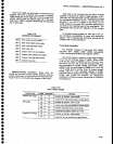
DB0-This
line carries
the
serial
data that
selects
which input
signal is
to be
counted and what
n
numbers
to use
in
the
r-2n
counter. This data
is
foaded into shift
register U1022. DBO also carries
the
data
for
the
+N
counter in
the Phase
Lock
Syn-
thesizer
circuits.
7-82