


Theory
of
Operaton
-
4g4[l4g4Ap
Service,
Vol.
1
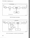
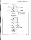
The
Synthesizer
can
be
divided
into
three
functional
blocks:
the 100
MHz
divider,
the
SO MHz
divider,
and
the
-+N
counter.
The
100MHz
divider
consists
of
flip-flop
UgOgOA
and
transistors
Q3040 and
e3041. The
100
MHz
signal
from
the
3rd
Converter
stags
is
applied
to
the clock
input
of
u3030A.
u30308
furnishes
a
stable
bias
source
for
the U3030A
clock
input.
The
signal
from
pin
3 of
U3030A
is
apptied
through
O3O4O
to
UtO+Og,
ine
50 MHz
divider. The
50
MHz
signal
trom
the
e
output
is applied
through
buffer
amplifier
e3041
to PSOO
{not
used in
this
instrument).
The
two transistors provide
ECL
to
TTL
level
shifting.
The
50
MHz
divider
consists
of
the flip-flop
U10408.
The
5O
MHz
signat
from
e3040
drives
the ctock
input
of
Ul0408, which
divides
the
signat
to 25 MHz.
The sig_
nal
from
th€
Q
output
is sent
to the
Offset
Mixer
cir_
cuits.
The complement
signal
is apptied
to the
+N
counter.
The
r-N
counter
consists
of shift
regist€r/latch€s
U2020 and
U2030;
counters
U2010,
U1O2O,
and
U1030;
and
flip-flop
U1040A.
The
circuit
is
controiled
by three
signals
from
the microcomputer
via
the
Counter
board.
The output
of
the
+N
counter
is
the
+N
fr€quency,
which
is applied
to
the
phase/frequency
detector
in
the
Offset
Mixer.
The
three counters
connect
to form
a 12-bit
counter,
overflowlng
after
a
count
of
4095.
When phase
lock
operation
is
selected,
the microcomputer
sends
serial
data
and a
data
clock
to
load
a
number
into
the latches.
The
number
ranges
from
3300
to
ggg0,
so
the
count
remaining
until
the counters
overflow
is from
265
to
795.
The 25
MHz
counter
clock
is
divided
by
the count
remaining
to
produce
the
+N
frequency.
At
power-up
and other
times when
not
phase
locked,
the counter
is
allowed
to count
to
4095
for a
6
kHz
output.
When
the number
is
loaded,
the
N LATCH
signat
transfers
the number
from
the input
shift
registers
to
the output
latches
ot
u202Q
and
U2030,
preserting
the
count€rs.
Once loaded,
the counters
count
at a 25
MHz
rate
to
accumulate
the remaining
number
of
digits until
they
are
full.
The
carry
output
of
U1030 (pin
15)
then
moves
high
and
U1040A changes
state.
This
reloads
the
counter
stages
with
a
new
number
for
another
count
cycle. The
carry
output
of
U1030
is again
simultane_
ously
set
low so
the
next
cycle
of
the 25
MHz signal
clocks
Ul040A
back
to
th€
reset
condition.
The
output
of
U1040A
is
a series
of
posltive
pulses
that
range
in
period
from
10ps
to
31
&s
which
is
equivalent
to 94
kHz
to
32
kHz.
This
signat
is
sent
to
7-84
the
phase/frequency
d€tector
in
the Offset
Mixer
for
comparison
with
th€ difisrence
frequency
generated
in
the
mixer
circuit.
Phase
Lock
(Diagram
40)
The
Phase Lock
circuits lock
the
lst
LO,
using
the
Synthesizer as
a reterence.
The circuits
shown
on
this
diagram include
the Ofiset Mixer
(A50A3,
Error
Amplifier
(A50A4),
Controlled
Osciilator
(A50AS),
and
Strobe Driver
(A50A2).
The
lst
LO
(A16)
and
the Phase
Gate Detector
(A24)
are also
maior
parts
of
the
phase
lock circuitry.
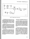
Offset Mixer. The
Offset Mixer
(A50A3)
circuits
mix
the
synthesizer
and VCO
outputs and
compare
phase
and frequency
with
th€
divid€-by-N frequency
from
the
synthesizer.
The resulting
error
signal
drives
the inner
loop amplifier
on
the Error Amplifier
board
(A50A4).
The circuits
consist of
a ring
diode mixer,
differential
amplifier,
and
phase/frequency
detector.
For
this expla-
nation.
assume
that
the Controlled Oscillator
(VCO)
fre-
quency
is at 25.06 MHz and
the
+N
signal
is
50 kHz.
The 25.06 MHz
signal from
the
VGO enters
the
board
at
pin
N
of
the Offset Mixer assembly. The
signal
drives
the
base
of
transistor Q2021
which
drives transformer
T2010. The
transformer
output
connects across
the
ring
diode mixer. The 25 MHz reference
frequency
is
applied
at
pin
K of
the
Offset
Mixer and coupled
through T1010
to the
ring
diode
mixer. The four
fre-
quency
components are
picked
ofr
at th€
cent€r
tap of
T2010.
A low-pass filter
pass€s
the 60 kHz difrerence
frequency
and
blocks the two
fundamental
frequencies
and
their
sum.
Transformer
T2030 couples
the 60
kHz signal
to
differential
pair
Q1020
and
01030.
Then
Ql040
amplities
the
signal
to
TTL levels and applies it
to
the
clock
input of
flip-flop U10508,
part
of
the
phase/f
requency
detector.
The
phase/frequency
detector
consists of flip-flops
Ul050A
and
U10508, NAND
gate
U20508,
and inverter
U2050A.
Now, if
the
loop
had bEen locked, the two
flip-flop
clock input signals would have
been
edge-
coincident. Pin 4 and
5
inputs of
U20508
would have
moved
high
and
after the
signal at
TP1058
goes
low,
the
NAND
gate
would have reset both
flip-flops. This
results in
a
series of
pulses
of equal amplitude and
width
from each of the
flip-nops
which,
when applied to
the Error Amplifier,
would
not shift the
frequency
of
the
vco.
However, in
this
example
the
+N
signal is
50
kHz
and
the difference
frequency from
Q1 040 is 60
kHz.
Thus,
Ql 040's
output
leads the
+N
signal. In this
case,
o
a
o
o
o
o
o
e
o
o
o
C
o
o
o
o
o
a
I
o
a
o
e
o
o
o
o
o
o
o
o
o
o
o
o
t
o
o
a
o
O
o
o
o