


o
o
o
I
a'
a
o
I
o
a
o
I
o
o
o
a
o
o
t
,
I
o
o
I
a
I
)
o
I
o
a
o
I
o
t
I
O
I
a
o
o
o
o
o
.
The
10
MHz
input
signal
from
the
VR
circuits
drives
input
preamptifier
e2075,
in
th€
tog
lmftiner
circuits
on
A62A1.
-
The
input preamptifier
ir"nsier"
the
S0O
input
signal
to
the high_impedance
input
of
the
first
amplifier
stage.
The
input
signal
is
ilso
apptied
to
transistor
01 07S,
a
common-base
amplifier
that acts
as
a
bufier
to supply
the
l0
MHz
lF
signat
to
the
rear_panel
connector.
..
Frgm
the
input
preamplitier,
the
signat
is
apptied
through
seven
cascaded
stages
each
cinsisting'ot
an
emitter
follower
driving
a
common
base
amptifier.
Resistors
between
the
emitter
follower
and
the common
base
sections
determine
the
gain.
Diodes
switch
vari-
ous
resitors
in
or out
of
the
circuit
to vary
the
gain
for
different
input
levels.
All
of
the
"t"g"J
are
similar,
except
that
the
first
three
stages
"ontaii
an
extra
set
of
diodes for
an
additional
gain
itep.
All
stages
have
maximum
gain
for
low
amplitude
input
signals.
As
the
input
amptitude
increases,
the last
stage
switches
to a lower
gain.
For
further
increases
in
input
amplitude,
additional
stages
decrease
gain
back
to
-the
first
stage.
Then
the
second
set
of
gain-
switching
diodes
switches
into
the
first,
second,
and
third
stag€s
to reduce
the
gain
for
the
larggst
signals.
Typically,
when
the
input
levelto
the emitter
follower
in
th€ last
stage
is
less
than
60
mV
peak-to-peak,
the
transistor
conducts
enough
to maintain
fonrvard
bias
on
series
limiting
diodes.
The
10
MHz
signat
path
at
that
level
is
through
both
diodes,
a
capacitjr,
ani
a resistor
network
to the
common
base
section
of
ihe
stage.
The
gain
.of
the stage
under
these
conditions
is
ipproxi-
mately
10
dB.
-
As
the input
signal
voltage
increases,
more
current
llows
through
the left
diod€
to
increase
the reverse
bias
of
the right
diode.
This
sharply
reduces
the
stage
gain
to
unity.
The
signal
current
then
flows
only
in
the
lower
path
around
the
diodes.
This
change
takes
ptace
during
the
positive-going
portion
of
each
cycte.
tne
opposite
occurs
during
the
negative_going
pdrtion
of
the
signal
above
the
minimum
input
level.
As
the
input
signal
increases
beyond
the
point
at
which
the
gain
of
the final
stage
decreases
to
unity,
the
same
sequince
occurs
in
the
preceding
stage.
and
in
succession,
back
to
the
first
stage.
Theory
of
Operailon
-
4g4Ll4g4Ap
Servtce,
Vot.
l
Signal
levels
above
this
point
activate
the
second
tier of
gain
reduction
in
the
first
three stages.
These
stages
each
incorporate
a
second
set
of
diodes
that
r€duces
the
gain
by
another
7
dB. In
the
first
tier of
gain
reduction.
reduction
started
at
the last
stage
and
proceeded
to the first;
in
the second
tier,
the
reduction
starts
at
the first
stage
and
proceeds
to
the
third.
In
the first
three
stages,
the lower
diodes
are
for-
ward
biased
untit
the
second
tier
of
gain
reduction.
With
a further
increase
in
input
signai
level,
limiting
occurs
in
the same
manner
as
previously
described
and
results
in less
than
unity
gain
through
the stage
(approximatety
112r.
The
one-two-th6e
reducrion
sequence
is
established
by
the values
of
the
pull_down
resistors
at
the
cathodes
of
the diode
pairs.
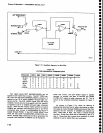
Detector
Circuit
This
circuit
demodulates
the 10 MHz
output
of
the
Log
Amplifier,
producing
the VIDEO
signal
that
drives
the Video
Amplifier
circuits.
The
detectoi
consists
of an
operational
amplifier
with
a
diode
detector
in
the feed_
back
path.
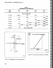
A low-pass
filter
at
the
output,
shown
on
diagram
23,
filters
the RF
from
the
dEtectlO
signal.
The
operational
amplifiEr
is
madE
up of
common
emitt€r
amplifier
01012
and a
differential
amplitier
that
consists
of
Q2010
and
e20l8. The
summing
node
for
the n€gative
input
is
the
base of
e1012
(the positive
input
is
at
the
grounded
emitt€r
of
el012).
The
differential
amptifier's
high
impedance
output
allows
it
to rapidly
change
during
the
period
when
both
detector
diodes are
effectively
open
circuited;
that
is,
when
the output
is
near
0 V. When
neither
diode
is
con-
ducting,
it
is necessary
that
the output
change
rapicfly
through
that
zone.
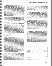
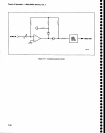
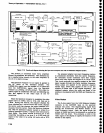
Figure
7-11
shows
a simptified
ac-equivalent
schematic
diagram
of
the
detector circuit.
Two
detector
diodes are
used,
but only
the negative
half cycle
is
taken as
the
output.
Ac coupling
is
used
on
both sides
of
the detector
diodes
to
prevent
ternperature
coefficient
effects
of
the operational
amplifier
from
affecting
the
detector
output.
The
detector
output
signal
is applied
to
the Video
Amplifier.
A
low-pass
filter
shown on
the
foilowing
diagram
compl€tes
the detector
by
filtering
the remain-
ing
RF.
7-31