


Theory
of
Operafon
-
494ful4g4Ap
Servtce,
Vot.
1
r
The
mixer
bias circuit
produces
and outputs
the
required
bias voltages
for
the 1st
Mixer.
.
The
programmable
bias circuit
provides
peaking
voltage for
the
Preselector
or external
mixers
bias
voltage
based on
data
supplied
by the
microcom-
puter.
Digital
Control
The
digitat control
circuit
controls
the
osciilator
span
volts, the
1st
Mixer
bias,
and
programmabte
bias.
Decoder U4034 output
1
(pin
14)
goes
low
when
the
input address is
72 and
output
Z
{gin
T)
goes
tow
for
address 7E.
When
output
1
goes
high,
data is
clocked
or latched into
U4017,
and
when
output
7
goes
high
data
is
latched
into
U4024
or
tJ4022,
depending
on
the
status of
data
bits DB6
and
DB7.
Data
for
U4017 eonsists
of control
codes for
the
oscillator drive circuits
and
the switches in
U1016,
which select
l st
Mixer
bias or
the
bias set
by
the
front-
panel
MANUAL
PEAKING
control.
The codes
are
described in Table
7-16.
Oata
at
address
7E
tor
U4022
and
U4024
drives
DAC
U3022
and
is
converted
to
an
analog
signal
which
provides
the
Programmable
Bias.
Input
Switching
lf
the
main coil
of
the oscillator
is not
to be
swept,
DBO
goes
low at
address
72.
This
cuts off
e3029,
de-
energizes K3034,
and
disconnects
the
SPAN VOLTS
signal to the summing
amptitier.
Diode
CR303t
pro-
tects 03028 from
the inductive
leedback
surges
that
occur at
turn-off.
7-68
Oscillator
Filter Switch Driver
When
DBO
is low,
relay K3034
is
de-energized and
02029 is biased
on which
drives a capacitor
switching
relay on
the 1st
LO Interface
board. The
capacitors
are
switched
acroEs the
main
coil,
when
it
is
not
being
swept,
to
lilter
noise riding
on
the tuning current.
capa-
citor
C2025
provides
a
gradual
decay
of
current
through
the r€lay
aft€r
power
is turned off.
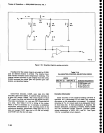
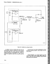
Summing Amplifler
Amplifier U2032 and
the
compl€mentary
pair
of
translstors,
02035
and
02039,
plus
related com-
ponents,
comprise
an operational
amplifier. The
COURSE
TUNE VOLTS ANd
thE
SPAN
VOLTS ArE
summed
at the
input
to u2032. The feedback
resistor,
for
the
operational amplifier, is Rl038.
The input
resis-
tance
is
R2O27
for
the
COARSE TUNE VOLTS signal
and
R20{}1
for the SPAN VOLTS signals.
(R2030
is
switched across
R2031
,
as mentioned
previously,
to
increase stage
gain
for maximum span operation.) The
output of
the
summing amplifier,
which can swing
from
-10
V
to
+10
V, is applied
to the
Preselector
Driver
cir-
cuits and
to the
Video Processor
board.
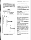
Oscillator Driver
The output
of
the
summing
amplifier also
drives
the
input
to the
oscillator driver
stage
when FET Q2040
is
switched on.
The oscillator
drivEr stage
consists
of
active components Q2045,
U2043, Q3047,
and Q352.
The input resistance
consists
of R2041, the
1st
LO
Sen-
sitivity adjustment
R1031,
plus
R2043. The feedback
resistance is R2042.
The arnplifier
bonverts a voltage input into a cunent
drive
for the l st
LO
tuning
coil
by
controlling
th€
voltage
across current
sens€ resistor R1040, which is in
s€ries
with the
oscillator tune
coil.
03047
assures that Q352
base
current remains within the
oscillator
tuning
coil
cir-
cuit.
Q2040
is biased
on except when
the
oscillator
is
degaussed.
The
summing
amplifier
output is applied
through the
1st
LO
Sensitivity
adjustment R1031
and
summed with an
offset
voltage set
by
the
1st LO Offset
adjustment R1032
at
the
input
to the
preamplifier stage
02045.
Adjustments
Rl031 and Rl032
match
the
oscil-
lator
driver
stage to the oscillator
characteristics,
R1032 adds offset to the
input of
the
preamplifier
to
place
the
oscillator
at center operating frequency
when
the
amplifier
input
is at
0
V.
02045
is a
low-noise, matched, dual transistor.
The
feedback
path
through
R3040 and R2042
sets
the
vol-
tage
across a
four-terminal resistor R1040.
This
vol-
tage
sets
the
current through
the
resistor which
is
also
emitter current for
driver transistor Q352.
The
1st
LO
Sensitivity
adjustment
Fll031, sets
the
voltage
gain of
o
a
o
o
a
o
o
o
o
o
I
o
o
o
a
a
o
a
I
o
a
o
o
o
o
o
o
o
o
o
o
a
I
o
t
o
o
o
o
o
o
O
o
O
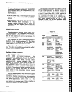
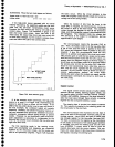
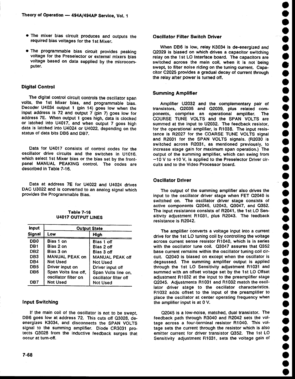
lnput
iiqnal
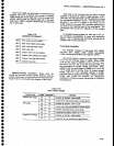
Table
7-16
U4017
OUTPUT
LINES
State
DBO
DB1
DB2
DB3
DB4
DB5
DB6
DB7
Bias
1 off
Bias
2 off
Bias
3
off
MANUAL
PEAK off
Not
Used
Driver
input off
Span
Volts
line on,
oscillator
filt€r off
Not
Used
Bias 1
on
Bias
2
on
Bias
3 on
MANUAL
PEAK
on
Not
Used
Driver
input
on
Span Volts
line
off,
oscillator
filter
on
Not
Used