


o
o
o
o
o
o
o
o
o
o
a
o
o
o
o
O
o
o
o
o
o
o
o
o
o
o
o
o
O
o
o
o
o
a
a
o
o
o
o
o
o
o
a
o
U10418.
Also,
when
th€
ON/OFF
tine
goes
high,
it
€nables
the
|NCR
gate,
UlOgTC,
to steer-the
poiition
counter
onto
the character
RAM
address
inputs
through
fine
driver
U3042
and
muttiptexers
UI050
and
U1046.
When
cleared,
this
bit
places
an
address,
latched
in
U3038 and
U3034,
on
the
character
RAM
address
inputs.
Bit
1 interprets
data sent
to
the address/data
port
as
an
address
(1)
or
data
(0)
for
the character
RAM.
Setting
this
bit
disabtes
the character
RAM
for
input
and
sets
up
the clock
signal
to latch
the address.
When
this
bit is set,
eg of
U0034
gates
a
high
on
the output
ot
U2044A.--This
high preue-nts
input
to
the
character
RAMs,
U20SZ
and
U2052,
by setting
its
R/W
input
high.
This
high
atso
disconnecti
the
instrument
bus from
the
character
RAM
data
inputs
by
disabling
U3047;
meanwhile,
U2O}ZA
is
enabled
to
gate
the ctock
signal
that latches
the address.
The
positive
clock
tran-
sition
is apptied
to
U3039
when
DATA
VALID goes
fatse
at
the end
of
a
writ€
cycle
to
the addressldata
port,
releasing
2F.
When
this
bit
is
cleared
and
2F
is asserted,
U2O44A
enables
the character
RAM
for
input
and passes
the
data
through
U3047.
Theory
of
Operation
-
4g4[l4g4Ap
Service,
Vol.
1
OFF is forced
low
to
disable
the
sp€ctrum
display,
and
W1028E
forces
the current
boost
addition
to
be
dis-
abled.
Also,
U1016 is
disabled
so
that
the
marker
dot
is
not
displayed.
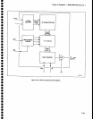
Address/Data
port
The
microcomputer
loads
char-
acters
for
crt
display
through
the
address/data
port.
Each character
requires
the
following
four
write
cycies.
1. Bit
2 in
the control port
is
set
for
an
address
transfer, and
th€ upper
2
bits
of
the
RAM
address
(A8,
A9)
are sent.
2. The
lower
I bits of
the address
in
the character
RAM
are sent
to
the
address/data
port.
3.
Bit 2 in
the
control
port
is cleared.
4. The
data is sent
to
the
address/data
port.
The
bits
are
defined
in
Table
7-10;
Bits
0-5 are
the
lower
six
bits
of
the
character
RAM
address
or
are
the ASCII
code
for
the
character.
Table
7-10
ADDRESS/DATA
PORT
Function
Address
of ASCII
code
Skip
bit
Blank
character
Bit
6
causes
the line
counter,
U2014,
to
skip
a line,
if set.
Bit
7 is
used to reduce
overhead
readout
display. lt
is set
when a space
is
transferred
to the character
RAM,
so
the readout
does
not
steal
time frorn
the
spec-
trum
trace
to scan a
blank.
When
set,
this bit
prevents
the GEN
RUNNTNG
flitrflop
from
gating
R/o
oFF tow
through
U2O44B.
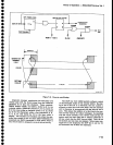
Frequency
Dot Marker
The
frequency
dot
marker
is refreshed
immediately
after
the last character position
in
the
lower
readout
is
scanned.
Normally,
the
marker
is centered on
the
screen
just
below
the upper
readout as a
pointer
for
the
center
frequency
readout.
When
MAX
SPAN
is
selected,
however,
the
dot marker
moves
to
a
point
on
the
display
that
corresponds
to
the
center fr€quency
value.
The
negative
transition
of line
D
triggers
the marker
generator.
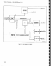
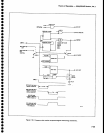
A simplified
diagram
of
the
circuit and its
timing is shown
in
Figure
7-22.
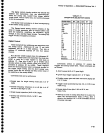
0
1
2
3
4
5
o
7
Table
7-9
CONTROL
PORT
Function
Readout
on/off
Address/data
A9
of
RAM
address
Max
Span
dot
A8 of
RAM
address
16
line
mode
40
characters/line
Spectrum
display
available
Bit
2
is
the MSB
of
the
RAM
address.
Bit
3 controls
the frequency
dot
marker.
This
bit is
set
in
the MAX
SpAN^m9de
to
position
the
frequency
dot with
MAX
DoT
CONTROL
from
the
Sweep
boarci
When
cleared,
this
bit centers
the frequency
dot on
the
spectrum
display.
Bit
4 is
the Ag
address
line
for
the character
RAMs.
Bit
5
is
the select
for
16 lines
mode.
Bit
6
selects
the
40
character/line
mode.
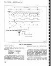
Bit 7 enables
the ctipped
display
with
the spectrum.
When
high,
U1055
is
enabled
and
causes.t40
ps
periods
to occur
between
characters
when
the spec_
trum is
disabled.
When
low,
U.l 05S is
disabled.
R/O
7-57