


Theory of
Operation
-
4g4[l4g4Ap
Servlce,
Vot.
1
ROM.
The
ROM in
this
instrument
is
located
on
this
board and on
th€
ROM Banks
& GptB
board
(A56).
The
ROM
consists of
system
ROM
containing
the
instrument
operating
system
and
the
program
RoM containing
the
various
measurements
routines
and
crt
messages.
The
system
ROM
is
always
accessible,
while
the
program
ROM
is
bank
switched
as
necessary.
Bank
switching
allows
expanded
memory
within
a
limited
address
space.
The system
ROM
and
part
of
the bank-switched
ROM
are
located
on
this
board.
The
remaining
bank-
switched
ROM
and
the
p6n1
switching
circuitry
are
located
on
the
GP|B
board (A56).
The
ROM lCs
are
32K-by-B
bit
erasable program-
mable
read-only-memories
with fifteen
addrees
lines
ancl
eight
data lines.
Each
contain
32K
bytes
of
data.
Normally,
the
ROMs
are
not
erased
or re-piogrammed.
U3050 includes
the system
ROM
and
one
bank of
th€ bank-switched
ROM.
The
ROM
frorn
C000-FFFF
is
the
system
ROM,
always
accessible
from
any
ol
the
bank
ROMs.
The
ROM
from
8000-FFFF
is
a
ROM
bank.
U2040C
and
U2040D ailow
both
the
g0O0
and
C000
address
selection
lines
from
LJ2O4S
to
select
the
same
physical
ROM.
The
two
halves
are
selected
by
address
bit
A14.
For
addresses
C000-FFFF,
A14 i;
high.
This address
range
is
also
enabled
through
U3030C and
U3030D.
For
the
bank
addrEsses,
9000-BFFF,
A14
is low.
Data
bit
D4 must
be high
when
stored at
the
bank
sefect
address,
7E00.
by tatch
U4020.
This
enables
U3050
through
U3030D.
U3060 comprises
ROM
banks
0
and 1.
This
lC is
:?le_cleq_lvhen
the
processor
addresses
the range
8000-BFFF and
when
the
CEO
signat
from
the GptB
board
(A56)
is
active (low).
Selection
between
banks 0
g."q
1
is
done by
the
bank.select
bit
latched from
D0
by
U4420.
This latch
is
enabted
when
the
BANK
signat
(ai
address
7E00)
goes
tow from
the
GptB
OoarO
1A56).
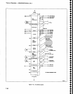
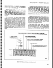
ROM
Banks
and
GP|B
(Diagram
43)
The
GPIB
board (A56)
contains
most
of
the
instrument's
bank-switch€d
ROM and
the
General
pur-
pose
Interface
Bus
(GPIB)
circuits.
The GptB
Interface
boarcl
{A30A5f
connects
the
instrument
to
the GptB
(IEEE
Std
488
bus).
On
the non-programmabte
version
of
the instrurnent,
this output
is only
used
to drive a
plotter.
'
Address
Decoder.
Decoder
U1O5S,
gated
by the
d2
Clock, is addressed
at
7800
by the t/O
line
from
the
Memory
board
(A54).
Address
lines
Ag-A10 produce
enable
signals
for starting
addresses
as
follows:
7-96
7400
for
the
9914A GPIA
7C00
for
th€
GPIB
Switch
Data
Buffer
7E00
for
the
ROM Bank
Select Enable
Bank
Selector.
Bank switching
expands
the
addressing
capabilities of
the microcomputer.
The
Bank
Selector circuit
allows addressing
272K
of
ROM
in
seventeen
16K banks. Each ROM
lC holds
two banks
in its
32K
bytes
of memory.
Banks
0,
1,
and
16
are
located on
th€
Memory
board
(A54).
Banks
2
through
15
are located
on
this
board.
Latch
u2044
reads
th€ data bus
at
address
7E00.
8it
D4 selects
between
the
first sixt€en
ROM
banks
and
th6
seventeenth
ROM
bank
(located
on
the
Memory
board). When
high,
bit
D4 enables
U3050 on
the
Memory
board
(A54).
When low,
bit D4 enabtes
U1O40
on
this board.
When
the lower
ROM banks are
selected,
bit D0
selects
even
and
odd
banks by driving
the
most
significant
address line
on each ROM lC.
When D0
is
low,
the
lower
addresses
in
each
ROM
are
selected.
These
are
the
even
bank
numbers. When
D0
is
high.
the
upper
(odd
bank) addresses are selected.
Bits
Dl
through D4 drive
decoder
U1040. Bit
D4
enables
the
decoder, and
bits
Dl
through
D3
provide
the
chip
enable signals
for
the
ROMs.
When
a
bank is
selectEd,
it
is
addressed
in the
8000
through
BFFF
range.
lf another
bank is selected, new
data
is
written
to
the
Bank
Selector.
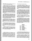
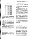
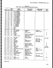
Table 7-23 lists
the ROM
set€c-
tion
data
for
the
lower sixteen
banks.
The
light-emitting-diodes
(LEDs)
on
U1040's
chip
enable
outputs
are
diagnostic
indacators. When
the
instrument
is
placed
in
a self-diagnostic
mode,
the
LEDs signal
results of
the
tests.
See
the Maintenance
section for
further
information.
Bank
ROMs. The
bank
ROMs
contain mosl
of
the
firmware.
This
includes
functions such as control
pro-
grarns,
rneasurement
routines, and crt
messages
{with
alternate languages
if
installed).
The memory lCs
are 27256 32K-by-8
bit
erasable
programmable
ROMs. They each have 15 address
lines,
I
data
lines,
a
chip
enable line, an
output
enable
line,
and a
program
voltage
line.
Normally,
the
ROMs
will not be erased or
re-programmed.
a
t
o
o
o
o
a
o
o
a
I
t
o
o
I
a
t
o
t
I
a
a
o
a
o
I
a
o
o
)
o
o
o
a
o
o
o
o
o
o
O
o
o
o