


o
o
a
o
I
O
I
a
o
o
a
o
o
I
a
I
O
o
I
a
o
o
I
a
a
o
O
O
o
I
o
o
I
O
o
a
a
o
o
o
o
a
o
o
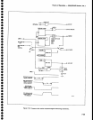
SPAN
ATTENUATOR
(Diagram
32)
The
span
Attenuator
selects
the
appropriate
attenuation
factor
for
the
incoming
swe€p
signal,
to
establish
the
frequency
span.
The
span
Attenuator
con_
s-ists
of
digital
control
circuits,
which
receive
and
decode
the address
and
instructions
from
the
micro-
comput€n
the
input
amplifters,
which perform
noise
reduction
and
signal
inversion
on
the
inioming
sweep
signal;
th€
digitat,to-analog
converter,
which
attenuates
the
sweep
signat
to
the
desired
amplitude
for
driving
the
l
st
LO
Driver
and
preselector
Driver
circuits;
ani
the decade
attenuator,
which
provides
three
decades
of
attenuation
for
the output
signals
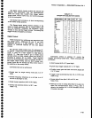
Digital
Control
Decoder
US025
decodes
the
address
information
from
the address
bus and
sends
a low
signal
to either
of
the
two tatches,
u1025
(address
75)
or
u2015
(gddress
76),
when
a
latch
is
addressed
anO
ttre
Oltl
VALID
lin€
rnoves
high. (Th€
data
is
stored
in
the
latches
on
the.trailing
edge
of
the
DATA
vALtD
signat.)
Logic
buffer
U4015
reduces
loading
of
the
data
bus.
Latch
U1025
stor€s
data
that contr;ls
th€
eight
least
significant
digits
of
the span
att€nuation
factor.
Latch
U2015 stores
data
that
controls
the
two
most
significant
digits of
the span
attenuation
factor,
and
other
functions
on
the
board.
When
a
span
attenuation
factor
is
selected,
the
microcomputer
selects
an address
and
pJlcg_s
the first
byte of
the
data
on
the
bus.
The
DATA
VALID
signal
causes
the
data
to
b€
stored
in
one
of
the
two latches.
Then
the
second
address
is
called
and
the
next
byt6 is
stored
in
the other
latch.
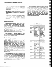
The
block
diagram illustrates
the
significance
of
each
bit in
tabtes
near
the affected
circuit.
A logic
1
represents
the
more
positive
of
two
levels
or
high
state,
and
a
logic
0
represents
the
more
negative
of
two
levels
or
low
state.
Input
Section
The
sweep
signal
and
its
ground
reference
are
applied
to differential
input
buffer
U3036.
Any
signats
or
noise induced
in
the
two signal
transmission
paths
are
canceled
by
this
stage.
.
The following
stage
consists
of
amplifier
UgO32,
plus
switching
transistors
e2025,
O2O2S:
and
e2023.
D.ifferent
rnixing
modes
require
the
2nd
LO frequency
to
either
increase
or
decrease
to increase
the
signat
ire_
quency.
Thus,
this
circuit
is a
unity
gain
amplifier
that
can
be changed
from
inverting
to non-inverting,
under
bus
control.
When
line
eg
of
latch
U2O1S
is
low-,
A2O2g
conducts
and
its
collector
moves
positive
to about
+5
V. This
in
turn causes
both
O2C'2S
and
e202g
to
conduct.
Pin
3
of
Ug0g2
is
effectivety
grounded,
the
sw€ep
signal
is applied
through
R3029
to the
summing
node of
the
amplifier,
and
the
gain
of
the stage
is
_1.
I
Theory
of
Opera0on
-
4g4Al4g4Ap
Servlce,
Vol.
1
fine
Q8
is
high.
O2O2g
do€s not
conduct
and
the
voltage
at
its
collector
fails
to
nearty
-1S
V.
Neither
e2025
n6r
Q2028 are
now
in conduction,
so
the sw€ep
signal
is
applied
to
pin
3 of
U3032. and
pin
2 is
disconnlcted.
Now,
the
gain
of
the
stage
is +i.
Digital-To-Analog
Converter
The
magnitude
of
the sweep
signal
is
determined
by
the
desired
frequency
span,
band,
and
option
InstalleA
in
the instrument.
The
microcomputer
calculates
the
proper
magnitud€
for each
combination,
and
sends
the
appropriate
codes
to
the
data
latches,
which
in
turn
control
the
attenuation
factor
of
the
digital_to-analog
convefter.
This
stage
consists
of
converter tJ1042,
ampfifier
U2A42,
and
a complementary
pair,
e2052
and
Q3056,
that
form
th€
output current
buffer.
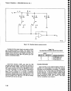
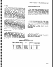
Figure
7-23
iilustrates
a
simptified
two-bit
digitat-to-
analog
conv€rter.
The
circuit
works
by current
division.
SincE
the summing
node of
the
amplifier
is
at
ground
potential,
the
magnitud€
of
th€ currEnt
through
a
resis-
tor is not
aff€cted
by the
position
of
the
switch
that
selects
that resistor.
For example,
when
switch
51
is at
position
B,
the
current
is
shunted
to
ground.
When
51
is at
position
A,
the current
through Rl
becomes
part
of
the total output
current.
Thus,
the
output
curr€nt
can
be
0, 1/4,
ll2, or
314
of
thg
total
cunent
available.
Because
of
the resistance
ratios,
th€ ratio
of
th€ output
voltage
to
thg
input
voltags
equals
th€ ratio
of
the out-
put
to the
total
curren!(Vo,r,/Vin
-
lout/lour).
In
this 2-bit
converteri
there
are
22 or
4 output
values
posslble.
In
th€ actual
lo-bit
converter,
there arc
21o or
1024 output
values.
fn converter
U10/'2, each
internal
resistance
is
switched
in
or out
by
a
CMOS FET
(internat
to the
dev-
ice).
The
CMOS
inputs
are
each
protEcted
by a series
input
r€sistor.
Since
the sweep
signal is
applied
to
th€
Vref input,
V1042 serves
as a
digitally controlled
attenuator
for
the
sweep
signal.
The attenuated
sweep
signal from
V1042 is applied
to U2042,
an operational
amptifier.
lt in
lurn drives an
output
current
buffer, consisting
of complementary
pair
42062 and
Q3056. The
pair
is
biased
to
produce
a
standing
current
of about
10 mA
in
the absEnce of
an
applied
signal.
This
eliminates
crossover
distortion of
the output
signal.
Diodes
CR2051,
CR2053,
CR1051, and
CR1049
pro-
vide
temperature
stabilization
for
the
bias current in the
stage.
When
high current
is
passing
through
the
pair,
diodes
CR1056 and
CR1061 clamp
the voltage
across
the emitter
resistors
to
reduce
voltage
drop.
7-65