


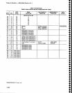

Theory
of
Operation
-
4g4Ll4g4Ap
Service,
Vot.
1
Secondary
& Fan
Drive
Circuits
(Diagram
47)
The
secondary
circuits
include
the rectifier_filter
cir-
cuit,
which
rectifies
and
filters
the
secondary
voltages;
the voltage
reference
circuit,
which
furnistrei
a
stiOte
and
precise
reference
for
the regulators;
and
the regula-
tor
circuits,
which
control
the
voltage
and
currEnt
lor
the supplies
that
require
precise
regulation.
The
Fan
Driver
board (A30Al)
contains
the Fan
Driver
circuit,
which
furnishes
the appropriate
drive
current
for
the
fan
motor.
lt also
contains
the
Over-
Voltage
Protection
circuit,
which shuts
down
the
+5 V
supply
in case
of over-voltage.
Reclifler-Filter
Circuits
Transformer
T4071
has
three secondary
windings.
The first
furnishes
current
to
the
+3OO
V and
+100
V
supplies;
the
second
furnishes
current
to
the
-7
V,
+7
V,
and
+9
V supplies;
and
th€ third
furnishes
current
to the
+17V
and
-17
V supplies.
The
linear
regulated
supplies (+5
V reference,
+5 V,
-5
V,
+iS
t, and
-1
5 V)
derive
their cunent
from
the rectifier-filter
cir-
cuits.
The
ac
voltage
from
pins
7
and
g
of
T4071
is
qp]i"_q
to_
a
bridge
rectifier
composed
of
CR3053,
CR3056,
CR3055,
and
CR3054.
The
output
of
this
rectifter
is filtered,
then
applied
to
the r€mainder
of
th€
lnstrument
as
the +100
V supply.
.
The
+300
V supply
is
derived
by stacking
a 2X
multi-
plier
on
the
+100
V
suppty.
CR3O52,
CRiO42,
CR1O34,
CR1022
and
associated
capacitors,
compose
this cir-
cuit.
-
The ac
voltag€
from pins
9 and 10
supply
current
to
full-wave
rectifier
CR4061/CR4062.
The
output
is
fltered
and
sent
to
the
rest of
the
instrument
as
the
*9 V supply.
Two
other
taps off
the same
winding
(pins
11 and
12)
supply
current
to
the
bridge
rectitier
ihat
consists
of
CR4063,
CR40S7,
CR40S3,
and
CR4065.
The
output
dividEs
across
filter capacitors
C9051
and
C4051
to
become
the +7
V and
-7
V
supplies.
The
+7
V
supply
is
only
used
on
the
Main
power
Suppty
board;
the
-7
V
suppty
is
used
by
other
circuits
in
ihi
instrument.
. .The
third
winding
of
T407.1 (pins
13,
14,
and
15)
fur_
nishes
current
to
full-wave
bridge rectifier
CR5052,
CR5062,
CR5065,
and
CR5055.
The
output
is
divided
to
bEcome
th€ +lZV
and
-17V
supplies.
The
-lZV
s.upflyl:
used onty
on
the
Main
power
Supply
board;
the
+17
V supply
is
used
both on
the Main
eower
Sup_
ply
board and
elsewhere
in
the instrument.
+5
V
Voltage
Reference
Supply
The +17V
is
divided down
by a
voltage
divider
to
Zener
diode
VR6026. The
6.2
V
from VR6026
is
divided
across
R6029,
R6028, and
R6023.
CR5031
provides
a
regulated
source
of bias
to
VR6020
after
+15
V
comes
up. The
+5 V
REF adjustment,
R6028,
is
set
by moni-
toring
the
+15v
supply and
setting
it tor
a
precise
+15.00
v.
Regulator
Circuits
The
+15V,
-15V,
+5V.
and
-5V
are
regulated.
Since all four
regulators are
basicalty
the
same,
only
the
+5
V regulator
is
described.
Significant
differences
are
discussed
following
this
description.
U2O37A,
the voltage regulator
part
of
the
circuit,
compares
the +5
v^g. and +5
v
sENsE
voltages,
amplifies
the difi€r€nce,
and applies
the change
to
driver
transistor
Q2023.
The change
is amplified
by
this
stage and
applied
to
the
base
of
seriss-pass
transistor
Q2024 to change
its
conduction
and
correct
for
the ori-
ginal
change
to the +5
V.
The +5
V sense
samples
the
+5
V at a
distribution
point
on
the
Mother
board.
This
signal
compensates
for
voltage
(lR)
losses
to that
point.
U20i!78 is
the curent limiter
portion
of
the reguta-
tor. The
amplifier
det€cts the voltage
differential across
the current sensing
resistor R2017, which
is
in seri€s
with the
output
load. When
the overload
threshold
is
reached,
as set
by
R2017,
R2039, R3032,
and
R3031.
U20378 removes
bias
current
from
driver
transistor
02023 and
Q2024. The
negative
bias on R3031
ailows
the limiter
to
rernain active
under short circuit
condi-
tions.
The +15
V regulator is
identical
to the +5 V
regula,
tor, except
that the ounent
limiter,
U2O37D supplies
additional
positive
bias
for
Q2031
when
it is not
active.
The
-15V
regulator
is
virtually
identical
to the +5V
regulator.
The
-5
V
regulator differs from
the others
in
that a
driver stage is not required,
so
the
preamplifiers
clrive s€ries-pass
transistor Q501
3 directly.
*5
V
Over-Voltage
Protection
Circuit
Zener
diode VR1015
and
SCR 01010 form the
over-voltage
protection
circuit. lf
the
+5
V supply
exceeds
+6 V,
th€
potential
on
the
gate
of
01010
biases it into conduction. This
forces
the
+5 V oupply
to
ground
potential;
it remains at
ground potential
until
the
mains
power
is
turned
off
and
turned
on
again.
o
o
o
o
o
a
o
o
o
o
a
o
o
o
I
o
o
o
o
o
o
o
o
o
o
o
o
o
o
o
a
o
o
o
o
a
o
o
O
o
o
o
O
o
7-106