


Theory of
Operation
-
494Al4g4Ap
Service,
Vol.
1
lf
the PwR FAIL
line returns
to a
high state
before
the
microprocessor
is reset,
the
microprocessor
does
a
power-up
initialization
to ensure
that
the instrument
operation will not
be
affected
by
a
temporary
power
loss.
This
power
fail
sequence
can
be
disabled
by remov-
ing
jumper
W2035. This
may
prevent
lalse
resets
when
operating
the
instrument
on
noisy
power.
However,
power-down
settings
will
not
be stored.
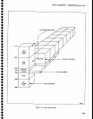
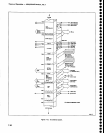
Memory
(Diagram
42)
The M€mory
board
(A54)
contains
some
of
the
ROM
and all
of the RAM
used
by the microprocessor.
There
are
64Kr
bytes
of
ROM
in
two
g2K
byte EpROMs
and
32K
bytes of RAM in
four
8K
byte RAMs.
Battery
backup
power
is supplied
for
16K
of
the RAM.
The
board
also
contains
the
Options switch,
which
sets
some instrument operations
and selects
processor
test
modes. Additional
ROM
is located
on
the
GplB
board
(As6),
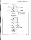
Address Decoders.
The address
decoding
circuits
rnonitor
the
microcomputer
bus to enable circuits
on
the
board.
Decoder
U2045
is
the main address
decoder,
selecting four
16K-byte
blocks
of address
space:
0000€FFF for
RAM
4000-7FFF for
NVRAM
and t/O
8000-BFFF for
Bank ROM
C000-FFFF for
system
ROM
The upper half of
U2045
decodes
the
non-volatile
RAM
and l/O space. The
lower
half
decodes
th€ system
RAM and
the ROM space.
The
OZ
Clock signal
ctocks
the
lower
half of
U2045
to
assure
proper
memory
tim-
ing.
The system
RAM
address space
is
the 16K
bytes
from 0000€FFF. The
2K
space from
7000-77FF
is
switched
b€tween eight
2K banks of
the 16K non-
volatile RAM.
The system
RAM
address space
is
divided
between
two 8K RAMs, U101O
and
U3020.
The
lower
half of
U2045, U3030C, and
U3030D
enabte
U1010 for
the
address
space
between
0000
and 1FFF.
The
lower half
of
U2045
and
the
upper
half
of
U3025
decode
addresses from
2000€FFF.
This enables
U3020.
The non-volatile
RAM
is
bank
switched
into
eight 2K
banks
addressed from
7000
throughTTFF.
This
allows
more
rnemory
than the
processor
can
directly
address.
At address
7E00,
the
bank select circuit
on
the GplB
board
(456)
enables
tatch
U4020.
The tatch
hotds
the
lx-m;o24-
7-94
RAM
bank number from bits D+D7 of
the
microcom-
puter
data bus.
LatchEd
bit
D7.
tne
62
and
the
7000 address
enable
from
the
upper
half of
decoder U3025 drive the lower
haff
of U3025
for
the
7OA0-77FF addr€ss space.
lf D7
is low,
U1030 is
enablEd; if hlgh,
Ul020
is enabled.
The
other
two bank
select bits,
D5 and
D6, directly drive
two
address
lines,
creating four banks in each of
the 8K
RAMs.
The l/O space
is
decoded
by
the upper half of
U2045, U3040,
and
U3045.
The
upper
half of
U2045
enables
U3040
for addresses from 7000-7FFF.
U3040
then decodes the
7800-7FFF
address tor
Options circuit
and other
l/O space.
This llne
is
sent
off
the board
as
the
l/O
signal.
The
Options
circuit is
addressed at
7800
by U3045.
ROM address decoding
is
performed
by the
lower
half of
U2045, data bit
D4, some
gates,
and
the bank
select circuits on
the
GPIB board
(A56).
Half of ROM
U3050
is addressed
as
bank
ROM
from
address
8000
through
7FFF. The
other half
of
U3050
is systern
ROM
addressed at
C000
through
FFFF.
The bank ROM
address space is shared
with 16 other ROM
banks.
Latch U4020
stores data
bit D4 at address
7E00
{Bank
enable).
When that bit
is high,
and
when
ths
ROM
banks
are
addressed, U3050
is selected. The
latched
bit
enables
U3050
through
U3030D.
For system ROM
addresses,
thg CXXX
enable
through
U3030C
and
U3030D,
and through U2040C
and
U2040D
enables
u3050.
U3060
is selected
as
banks 0
and 1 by the
bank
select circuit on the
ROM Banks and
GPIB
board
(A56).
The
upper
and lower
addresses are selected by
data bit
D0 latch€d
by
uao20
at
address
7E00.
RAM.
The
RAM
is divided
into systern
RAM
and
non-volatile RAM.
The
microcomputer uses the
system
RAM
for
interim data
storage while the
instrument
is
operatang. The non-volatile
RAM
stores
changeable
data
such as
waveforms,
readouts, and front-panel
set-
ups.
The
non-volatile
data is
backed
up
by
battery
power
when the
instrument
is not operating.
U1010
and
U3020
form th€ main
system
RAM.
Each
lC contains 8K bytes
of
RAM,
making
16K
bytes
totalsystem
RAM.
U1020
and U1030
form the
battery-backed-up
non'
volatile RAM.
When
the
instrument
is operating,
these
RAMs
are
powered
by
the +5 volt supply.
When
the
instrument is
not operating, the RAMs
are
powered by
a
o
I
o
o
a
t
O
o
a
I
o
o
o
o
o
a
o
I
t
a
o
a
a
o
I
o
o
a
o
I
o
o
o
o
o
a
o
o
o
o
o
I
o