


Theory of
Operation
-
494A/4g4Ap
Service,
Vol. 1
Clock.
This
circuit
generates
the
clock
signat
that
drives
the
microprocessor,
the
GplA
transceivdr
on
the
GPIB board
(A56),
and
the
character generator
circuitry
on
the
CRT
Readout
board (A66A1).
Y1030,
Q2035,
and
e1030 form
a clock
circuit
that
oscillates
at
3.4133
MHz.
e2095 and
y1030
form a
Colpitts
oscillator
and
el030
buffers
the output, giving
a TTL
compatibte
ctock
signat.
This
signat
is
turtnei
buffered by
U2030A
forming
th€ crt clock
signat.
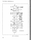
Mlcrocomputer
Bus.
Microcomputer
communica-
tion with memory
and l/O
is via
the microcomputer
bus.
The
bus consists
of eight
data tines (D0-Dti),
sixteen
address
lines
(A0-A15),
the RESET
tine,
the
VMA (Vatid
Memory Address)
tine.
the Read/Write
(R/W)
tine,
and
the
62
Clock.
The
data
lines
connect
from
the
microprocessor
through bi-directional
buffer
VZ02S.
The
Read/Write
line controls
data
direction
through
the
buffer,
When
the
microprocessor
releases
the address
bus,
the
Bus
Available
line
(BA)
disables
the
data
bus
buffers
through
U3036A.
Jumper
P3015
is
a
test
jumper
that
ailows
disabling the
data
buffer and
forcing
a
CLR
B
instruc-
tion to
the microprocessor.
Diodes
CR2O20
and
CR2025
pull
data
tines
MDS and
MD7
tow,
issuing
the
CLR B instruction.
The address
lines
connect
from
the microprocessor
through buffers
U3030 and
U302S. These
buffers
are
disabled when
the
DMA
Controller is
granted
the
address
bus.
Then
the addresses
come
from
the
DMA
Controller,
U1020,
through
DMA address
buffers
U1015
and
U1024.
U1015 is a
bi-directionat
bufier,
allowing
the
microprocessor
to
address
the
DMA
Controiler.
The RESET
signal
is
a function
of
the
power
Failure
circuit.
When
a
power
failure
is sensed,
the
RESET
sig_
nal
resets the
Timer,
PlA,
DMA
Controlter.
and
circuits
on
the Memory
(A54)
and
cptB
(A56)
boards,
The
Power
Fail circuit
is
discussed
in
more
detail
later. The
VMA, R/W,
and
02
Ctock
signats
have
atready
been
described.
Address
Decoder.
AU303S
decodes
the
addresses
for
the
l/O circuits
on
this
board. When
the micropro-
cessor
selects
an
address
in
the
range
of
7g00-7FFF.
the
l/O line
from
the Memory
board
(A54)
goes
low,
enabling
U3035.
The
decoder
then subdivides
the
address
range
to
select
each circuit.
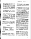
Figure
7-3.1
shows
the
UO
address
map.
Each circuit
uses
only
one
or a lew addresses
within
its range.
7-92
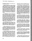
Tlmer.
The
Timer
circuit,
U2015, is a 6840
program-
mable
timer
used by the microprocessor
to
generate
variable
time
delays. The
processor programs
an
inter-
val into
the timer. When
the
interval
passes,
the
Timer
generates
an
interrupt
fl-imer
SRA). The
{2
Clock syn-
chronizes
the Timer
with the microprocessor.
An
address
in the
timer
range selects
the Timer.
Address
bits A0-A2 select
internal Timer
registers,
count€rs,
and
latches.
When
the
ReadfAlrite
(RfA/)
line
is low,
the
Timer accepts
data
input from the
data
bus.
When
the
line is high,
the Timer
puts
its
data
on
the
data
bus.
See
a
6840
data sheet tor
additional details.
The Timer
addressing is
mapped in Figure 7€2.
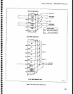
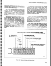
PIA and
Instrument Bue.
The microcomputer
com-
municates with
the instrument
through the
lnstrument
Bus.
The
6821 PlA,
U1010,
interfaces
the
DigitalControl
circuits
to the
Instrument
Bus.
This
bus
contains
eight
data
lines
(DBO-DB7),
eight address lines
(AB0-A84,
the DATA
VALID
line,
the
Service
Request
(SER
REQ or
SR) line, and
the
POLL line, allthrough
the PlA.
The PIA
receives Read/'li/rite,
02
Clock,
and RESET
control signals
from
the
microprocessor. Figure
7-32
shows the
PIA
address
map.
The
address
lines are buffered by
U3015. The data
lines
are
buffered
by
bi-directional
buffer U3010. The
buffer
is
gated
on when
data
is valid.
The
most
significant address
bit selects data direction so
that
half
of
the
address
space is
for
writing
to the
instrument,
and half is
for reading from the instrument. The PIA
CB2
port
(U1010
pin
19)
goes
low when
the data on
the
lnstrument
Bus is valid. Resistor-capacitor circuits
delay the
DATA
VALID signal to the
Instrument
Bus.
assuring
the
proper
timing
relationship with
the
other
Instrument
Bus signals.
The
PIA issues
the
POLL and DATA
VALIO
(or
DV)
signals in
response
to
a
service request from
the
hardware on
the
Instrument Bus. The requesting circuit
responds
to
the
POLL signal on the Instrument
Data
Bus.
The Internal
Control
(INTL
CONT)
signal comes from
the
Accessories
Interface assembly
(A30A76).
This sig-
nal
is
normally high
unless
external
control
through
the
ACCESSORIES connector is desired. When
low,
the
Bus
Enable
signal
goes
high,
disabling
the address
and
data buffers
and
the
DATA VALID
and POLL outputs.
The Bus
Enable
jumper,
P3010, may be
removed
to
dis-
able
the
Instrument Bus for
test
purposes.
DMA
Controller.
When the instrument
transfers
data
through
the GPIB
interface,
the DMA Controller,
Ul020,
sets
up direct
transfers between
system RAM
and the