


Theory of
Operation
-
494A/494Ap
Servlce,
Vol. 1
After
mixing,
the
l0MHz
output
signal
is
fittered
with a second
monotithic
crystat
fitter (y2020).
This
filter is
important
to
the
system
operation.
Without
it,
a
large
signal
at
9.75
MHz
woutd
be
present
in
the
wide_
band
VR amplifiers
that
foltow.
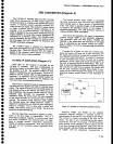
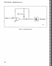
Local
Osclllator.
The
Local
Oscillator
assembly
(469A4)
provides
the 9.75
MHz square
wave
LO signali
needed
for mixing.
This
is
derived
from
a
19.S MHz
9ry_sFl
oscillator
by
using a
duat
D-type
flip-flop
in
divide-by-two
circuits.
Since both
sections
are
avail_
able,
one
is
used for
each
mixer.
This
provides
excel-
lent isolataon.
One output
drives
the
buffer amptifier
to
!he.11
Mixer
(A69At),
and
the other
dir€cfly
drives
the
2nd
Mixer
(A69A3).
A +5
V
regutator
on
this
board
powers
the
flip-flops.
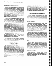
10 dB Gain
Steps
(Diagram
20)
The 10
dB
Gain
Steps circuit
provides
system
gain,
a 10 Hz
gain
adiustment,
a
10
dB switchabti gain
itep,
and the front-panel
overall
gain
(AMpL
CAL) control.
The circuit
consists
of
three stages
of
amplification.
The nominal
input
signal level
from
the 1st
Filter
Select
carcuit is
-25
dBm
for a
resolution
bandwidth
of
100 kHz.
(All
levels
listed
in
this
description
relate
to
the
100
kHz resolution.)
The
input
signat
is apptied
through
impedance
transformer T4019
to
the first
amplifier
stage
consisting
of
a
differential
pair,
0301
6 and
e2027,
driving emitter
follower
01036.
The
signal
feeds
back
to
the base of
Q2027 through
divider
R2034
and R20S1.
Signat outpui
resistor R2035
presents
approximatety
S0 ohms output
impedance
to the next
stage.
Gain
of
th€ input
stage
is
the same
for
all
resolution
bandwidths €xcept
10H2.
When
10Hz
is selected,
Q2015
connects
10
Hz
Level control
R2025
and R3029
across
R2031.
Tle
lst stage
output
drives common
emitter
stage
02043. Gain of
this stage
changes
by
+10
dB
when
Q4039
is switched
on.
Data
bit
0
froni
the
gain
steps
decoder
circuit
on
the
VR Mother
board
#2
{A6gA2)
controls
this
galn
step.
When
the
bit is
high,
emitter
resistor
R2048
sets
the
stage
gain.
When
low.
e40gg
saturates and
shunts
R2049
with
R3039
and
10
dB Gain
adjustment
R3035.
This
increases
the stage
gain
by
10 dB.
The output
of
Q2043
drives
the input
of
the
third
amplifier
stage.
This
stage operates
the same
as the
first
stage
except
the
gain
is adjustable
by
the
front
panel
AMPL
CAL screwdriver
control.
plN
diode
CR1053
and
resistor
R1056
shunt
resistor
Ft1060
to
7-26
control
the
gain
of
this stage. The AMPL
CAL control
biases CR1053. The
amount of current
through
the
diode
determines
its
high-frequency resistance.
As
the
current
through the
diode increases.
the resistance
decreases
and the
gain
of
the
stage
increases.
Gain
range is approximately
14
dB.
Output
impedance
of
the
stage is
50 ohms
as set
by
resistor
R1064. Nominal
output
level
is
-1
dBm for
a
full
screen
display. This level may
be as high
as
+9
dBm
when
MIN NOISE
is active. In
the MtN
NOTSE
mode,
'10
dB of att€nuation
is removed from
the
instru-
ment input step attenuator.
vR
Input signals
are
higher.
H€nce,
10 dB of
gain
is removed from
th€
VR.
20
dB Gain Steps Circuit
(Diagram
20)
This
circuit
provides
gains
of
-8
dB, +2
dB,
+12
dB,
and +22
dB in
precise
10
dB
steps.
The
nomi-
nal
-1
dBm
input
is supplied
through
pin
P from
the
10
dB Gain Steps
circuit.
This signal is
applied
to a
chain of
three
amplifiers,
each using emitter
degenera-
tion.
A change of
the
emitter resistance
changes
the
amplifier
gain.
The
gain
step
decoder
on
the
VR Mother
board #2
supplies
the switching signals
that
s€lect
the
amplifier
gain.
These
amplifters
are similar
to
the
10
dB
Gain
Step
amplifier
previously
described.
On this
board,
the
first
two
amplifiers are cascaded for
the
20 dB step
and
the
third
amplifier
provides
the
addi-
tional 10
dB
step.
The nominal
gain
of
the
compl€te circuit is
-8
dB,
with
th€
gain
steps switched
off.
This
provides
a nomi-
nal
-9
dBm
output.
In this
condition. control
pins
V and
Y
are
high, biasing Q2018,
Q204{
and
Q1062 off.
For the
20 dB
gain
step.
02018
and
Q2042 turn
on
(pin
V is
low),
increasing
the
gain
of
the
first
two
ampf
ifiers
by
10 dB each, for
a
2O dB
gain
step. Poten-
tiometer
A2029
(20
dB Gain)
adjusts
the first
stage
(O1025)
gain
shift while
the
second
stage
(Q1035)
gain
shift
is fixed at about
+10
dB.
The adjustment
allows
setting
the
gain
step
to
exactly +20
dB.
For
the
10
dB
step,
pin
Y is
low,
saturating
Q1062.
This raises
the
gain
of
the third
amplifier
(Q1043)
by
10
dB, as
set
by
R2060.
Gain
of
the 20 dB and 10
dB
gain
step circuits is
controff ed
by data bits 0,
1, and 2. Data
is
latched
on
the
output of
decoder U3017
on
the
VR Mother board
#2.
When the
bits are
high. transistor
04035, 03035,
and
Q4037
switch on. The resultant
low out
turns
on
the
respective
gain
step circuit.
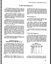
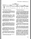
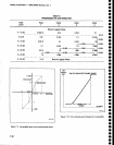
Table
74 shows
the
state
of
bits
2,
1,
and
0
and
the
gain
shifts obtained.
The output
signal from
the 20
dB
Gain Steps
circuit
is applied
through
a coaxial
cable
to the
VR Band Level-
ing circuit.
o
o
o
o
o
a
I
I
o
o
o
I
o
o
o
o
o
t
I
o
a
o
O
o
O
o
o
o
,
t
I
I
o
o
o
o
o
o
D
o
O
O
t
a