


a
o
o
o
o
o
I
o
o
a
o
I
a
o
o
a
o
O
o
o
I
o
o
O
I
o
o
o
o
t
,
o
a
o
I
O
o
o
o
o
o
o
I
o
amplifiers
provide
approximatety
+10
dBm
to
the
2072
MHz
2nd
Converter
and
+g
dBm
to
the
Reference
Mixer.
Sinc€
the
two
buffers
are..nearly
identical,
only
the
2nd
Converter
buffer
is
described.
'Oain
is
provicled
by
Q1011.
printed
elements
provide
input
and
ortpui
imp:91199
matching..
Out-of-band
damping
is
provided
by
R1011
in
series
with
a
t/4
wavelengih
snorted
stub.
Dc is
btocked
by
G1014
and
C101t.
i t1+
wavetength
open
stub
is
used
at
the output
to reflect
one
of
the
2;d
Converter's
image
freguencies
at
4ZS4
MHz (the
other
buffer
does
not
use
nor
need
this
stub).
Collector
bias
for
Q1011
is
provided
through
Rtfiz;
11011,
the 1/4
wavelength
shorted
stub.
and
R1011.
The
114
wavetength
shorted
stub
is
grounded
through
C2Oi
1
(C2011,
Cl0lg,
and
L1011
aie
also
used
for
decou-
pling).
Coilector
vottage
is
determined
by
divider
R101g
and
R2013;
this controts
the
dc
te6dback
to
the
collector-base junction
of
eloll.
The
bias
network
is
decoupted
from
the
RF
path
by
L1014.
Diode
CR2013
protects
the
base
of
el01
1
from
excessive
reverse
bias
if
the +12
V
suppty
fails.
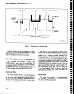
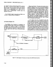
2200
MHz
Reference
Board (Diagram
t4)
_
Th,"
circuit generates
harmonics
of
the
100MHz
input.
The
22nd
harmonic
or
2200
MHz
is
used
by
the
Reference
Mixer.
The
input
100
MHz
signal
ls
apptieO
through
€^matching,network
lconsistiig
of
LiOg4,
L1025,
C1096,
C1029,
and
Clb2S)
to
i
oinerential
amplifier (01024
and
e2024).
The
€mitters
of
this
ampfifier
are
ac
coupled
through
C2026,
reducing
low
frequency gain
and
ensuring
balanced
operation.
A
snap-ofr
diode (CR2014)
is
driven
by
the
amplifier,
via
transforner
T201
5, to
generate
muitipte
harmonics
of
the 100
MHz
signat
inctuding
the
22Ob
MHz
reference.
The
output
passes
through
a
3
dB
attenuator,
for
isola-
tion,
to
the Reference
Mixer
circuit.
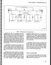
22A0
MHz
Reference
Mixer (Diagram
i4)
Signals
from
the 2200
MHz
Reference
circuit
are
filtered
by a
printed
22AO
MHz
bandpass
nner.
OioOei
CR1011
and
CR1012
are
the
switching
elements
of
a
single-balanced
mixer.
The
microstrip
Lscillator
output
is applied
to
CR1011
and
through
a
1/2
wavelength
deray rine
to
cRl012.
The
deray
rine
shifti
the
osciilator
signal
180
degrees
so
both
diodes
switch
together.
Mixing
the
2200
MHz
with
the osciilator
Z1g2
Mfiz
sig_
nal
produces
the
difference
frequency
of
1g
MHz.
This
18 MHz
signat
is
fed
through
a
3Z
MHz
tow_pass
fitter
to
th€ 16-20
MHz
phase
lock
circuit.
The
low-pass
filter
pley9lls
llwanted
products,
such
as
82
MHz (product
of
2100MHz
and
21g2
MHz),
from passing
into
the
phase
lock
circuit.
Theory
of
Opera{on
-
4g4Ll4g4Ap
Servlce,
Vol.
1
16-20
MHz
Phasetock
Board
(Diagram
13)
This
board
contains
regulated
pow€r
supplies,
a
16-20
MHz
(18
MHz
nominal)
voltage
controlled
oscilla-
tor with
linearizing
circuitry,
and
a
phase/frequency
detector
circuit.
lts
main
function
is
control
of
thi
2182
MHz
Microstrip
Oscillator.
Th€ entire
circuit
board
is
housed
in a
magnetic
shield
to reduce
spurious
efiects
of
external
ac
fields.
All
power
supply
and
con-
trol
inputs
enter
thg circuit
board
via
feedthrough
capa-
citors
in
the
housing
wall.
All connections
with
the
1ic^loyave
circu_rlry
are
through
feedthrough
capacitors
c2200
through
c22a4.
in
the floor
of
the ho=using.
The
+15V,
-lSV,
and
+gV
supply
inputs
are
re-
regulated
down
to
+12V,
-12V,
and
*5.2
V
by
regula-
tors
using operational
amplifiers.
lC
U2O2S
prbvides
a
stable
-6.2
V
reference
that is
fittered
by
R201g
and
C2015
and amptified
by
U20t6B
to
produte
the
-i2V
supply.
fC
U20168
uses emitter-foilower
e2024
to
increase
the
current
capability
of
the supply.
Resistor
R2013
ensures
sufficient
base
drive,
wiriie
collector
resistor
R2025
r€duces pow€r
dissipation
in
e2024.
Diode
CR2019
protects
the base-emitter
junction
during
power
supply
shutdown.
Feedback
resistors
R2016
and
R2017
set
the
gain
of
U2O16B
and
control
the
-12
V, +12
V, and
*5.2
V suppty
vottages.
..^-fE
-12V
suppty
is
apptied
to
inverting
amptifier
U2016A
to
produce
the +12
V supply,
and
inverting
amplifier
U1017
to
produce
the +S.2
V suppty.
The
out-
put
circuitry
for
the
+12V
and
+5.2
V supplies
are
simi-
lar
to
the
-12
V
suppty.
Differential
ampliffer
V2072A
accepts
th6 2nd
LO
sweep
voltages.
One input
senses
the
sweep
voltage
while
the other
input
senses
the
ground
potentiat
at
the
Sweep
board.
Sweep
sensitivity
is adjusted
by select-
ing resistor
R2070.
fn wide
spans,
the sweep
signal
passes
through
parall€l
resistors
R2AE2 and
R20g3.
ln
narrow
spans,
R2082
may
be switched
out
by 02094,
which
reduces
the weep
sensitivity
by
a factor
of
ten.
When
the TTL
signat
to
02026 is
high,
e2076 is
tumed
off,
R2086
holds
the
gate
of
e2094 to
-lS
V.
e2094 is
turned
off, and
R2082
is switched
out.
This
reduces
the
sweep
sensitivity.
When
the
TTL signal
is low,
e2026
saturates
with
the
collector
stighfly
above
0 V,
O20g4
turns
on, and
full
sweep
sensitivity
is restored.
Amplifier
U2072B
accepts
the 2nd
LO
tune vottag€.
the Tune
board
senses
the
ground
potential
of
the 16-
20
MHz
Phase
Lock
board
and floats
the
tune
voltage.
Tune
sensitivity
is
adjusted
by selecting
resistor
R2Ol2.
The
sweep
and
tune signals
combine
at
the sum-
ming
node
input
of
a non-linear
shaping
amplifier. The
non-linearity
of
the shaping
amptifier
compensates
for
the non-linear
tuning
of
the
reference
oscillator varactor
to
give
a
linear
tuning
characteristic
from 16
to
20 MHz,
The
shaping
function
is
produced
by
a resistor-diode
7-11