o
o
C
o
I
o
o
C
o
o
o
o
o
a
o
I
O
t
o
J
a
o
o
a
o
o
t
o
t
I
o
o
o
a
o
o
o
o
a
o
o
a
I
o
x
x
x
x
x
x
x
x
x
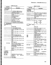
Data
Bits
7654321A
J.
Preselector
Driver
(77)
0lxxxxxx
l0xxxxxx
00xxxxxx
xxlxxxxx
K.
CENTER/MKR
FREQUENCY
Con-
trol
lxxxxxxx
0xxxxxxx
x0xxxxxx
xx0xxxxx
xxx0xxxx
xxxxxx0x
xxxxxxx0
DB7-DBO
D87
DBO
L. Auxiliary
Synthesizer
Control
(7D)
DB7-D84
DB2-DBO
synthesizer
chip
data
(D3-D0)
Synthesizer
chip
addresses
x0
xx
xx
XX
xx
xx
xx
xx
xx
X
1
0
x
x
x
x
x
xxx
xxx
xxx
lxx
0xx
xlx
x0x
xxx
xxx
NNNN
x
0 t
0
0 0 NN
x
01
1
0000x100
X
x
x
x
x
x
x
1
Mafntenanca
-
494A1494Ap
Service
Vol.
1
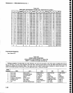
Table
6-13
(contl
Table
6-13
(cont)
Descrlption
-conversion,
g2g
MHz
ofiset
+conversion,
829 MHz
offset
829
MHz
tF
not
usEd
Driver
output
filter
on (for
narrow
spans)
Driver
output
filter
off
Preselector
switch
LPF
switch
lst
LO
FM
coil
not
swept
1st
LO
FM
coit
swept
Driver
on
Driver
ofi (for
degauss)
3rd
harmonic
1st
LO conversion
lst
LO
conversion
Control
(70)
1st
LO
storage
gate
open
1
st
LO
storage
gate
closed
Steers
DAC
data
to 1st
LO
high
byte
Steers
DAC
data
to ist
LO
mid
byte
Steers
DAC
data
to
1st
LO
low
byte
2nd
LO
storag€ gate
open
2nd
LO
storage gate
closed
steers
DAC
data
to
2nd
Lo high
byte
Steers
DAC
data
to 2nd
LO
mid
byte
Steers
DAC
data
to 2nd
LO low
byte
DAC
Data (71)
Data
for
center
frequency
DAC(s)
steered
by control
register
CENTER/MKR
FREQUENCy
Con-
trol
Read (F0)
1st
LO
DAC
stored
voltage
com_
parator
2nd
LO
DAC
stored
voltage
com-
parator
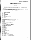
Data
Bits
76543210
L
Auxlllary
Syntheslzer
Control
(7D)
(cont)
0101x101
0000x110
0000x111
AAAA
x
0
0 0
000Ax001
M.
Phase
Lock
Control
xxxxlxxx
xxxxxxlx
DB6
DB2
DBO
lxxxxxxx
xlxxxxxx
xxlxxxxx
DB4-DBO
N.
Front
Panel
lxxxxxxx
0xxxxxxx
DB6-DBO
DescripUon
This
section
sets
R,
the reference
divider
to
5
yietding
a
20O
kHz
reference
frequency.
This section
sets
the
value
of A
from
0 to 31
LSB
This
section
sets
N
from
3.1
to
34
31-1111
32-0000
01
.r0
33*0001
34-0010
10
10
Write
(73)
Glocks
data
on
DBo
into a tatch
Clears
the
counters
Transfers
DBO
serial
data
to con-
trol
latch
outputs
Resets
the
counter
output
register
selector
Transfers
DBo
serial
data
to
syn-
thesizer
N latches
Gate mode
latch
NVRAM
switch
latch
Serial
data
for control
of
syn-
thesizer N latches
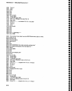
Read
(F3)-Most
Slgnlficant
Byte
Enor voltage
below
a
preset
amount
Error
voltage
above a
preset
amount
Valid
count
is
in
counters
Upper five
bits of
counter output;
the
remaining
16
bits
are
in
the
following
two
bytes
Reading
Data
Encoders
(F4)
CENTER/MKR
down
From
Swilch
FREQUENCY
CENTER/MKR
FREQUENCY
up
Switch
codes
(see
Figure 7-33
in
Section 7)
lxxxxxxx
xxlxxxxx
xxxlxxxx
xxxxlxxx
xxxx0xxx
xxxxx0xx
(A2-A0)
VCO
enable
xxxxlxxx
xxxx0xxx
vco
6-6r


