


back loop
for
U5030
is
now
open.
Diode
CR5035
turns
on
to
prevent
U5090
from
slewing
too
far
negative.
ldentily
Circuit
This
circuit
provides
a vertical
offset
on
alternate
lllcg:
t9 help
identify
truE and
fatse
signats.
When
the
'ldentify"
feature
is
in op€ration,
it
allolvs
the
operator
to
distinguish
between
responses
that
result
from
sig-
nals
at.
the desired
spectrum
analyzer
input
trequenjy
(true
signals)
and
those
that are
produced
by'othe?
spurious
or
harmonic
conversions
(false
signats;.
fatse
signals
shift
horizontally
on
alternate
trac6s
while
true
signals
remain
in
position.
The
horizontal
offset
is
accomplished
elsewhere
in
the
instrument
by moving
the 1st
and
2nd
LO
frequency
an equal
and
opposite
amount,
related
to
the ist
LO
harmonic
used,
or
by
moving
the lst
LO
twice
the lF
divided
by
the harmonic
number
(N),
on
every
other
sweep.
The
result
is
that any
conversion
pioducts
causing
a false
response
will
shift a
significant
amount
horizontally
on
the
display
while
true
signals
will
remain
close
to each
other.
The
identify
offset
circuit
described
here
shifts
the
alternate
or'ldentify"
sweep
vefiically
as a
further
aid
to
identify
th€ true
signals.
The
microiomputer
sets
DB6
high
during
'ldentify"
sweep
so
the
open
collector
out-
put
of
U4160A (pin
1)
goes
from
-15V
to open.
This
remov€s
the current
normalty
flowing
in
R51
54, R51
SS,
and
R5158
from
the summing
node
of
U5030
and
causes
a shift
in
the VIDEO
il output
lev€t.
Theory of
OperaUon
-
494A1494Ap
Service,
Vot.
I
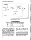
vtDEo
PROCESSOR
(D|AGRAM
24)
The
Video Processor performs
four
functions.
The
ftrst
is compensation
for flatness
variations
in
front-end
response.
The second
is
vldeo filtering,
which provides
the
selection
of
six
video
bandwidths (90
kHz,
O kHz,
300
Hz,
30 Hz.
3 Hz,
and
0.3
Hz)
under control
of
the
instrument
microcomputer.
The
third function
is
out-of-
band
blanking, which
blanks
th€
upp€r and
lower
ends
of
the
local
oscillator
swept
frequ€ncy
range
to
provide
a
selected
window
for
the
display. This
function
is also
controlled
by the
microcomputer.
The
fourth
is
the
capability
to
genErate
a negative-going
ditch
marker
on
the
video
display for
interfacing
with
a 1405
TV
Side-
band
Adapter.
Interface
with 1405
TV
Sideband
Adapter
The
TEKTRONIX
1405
W
Sideband
Adapter
is
a
specialized
tracking
generator
that is
used
with
the
Spectrum Analyzer
to
analyze
the response
of
a
televi-
sion
transmission
system.
The
Spectrum Analyzer
monitors
the
RF output
of
the
transmitter while
the side-
band adapter
drives
the
video
input
of
the
system.
The
video
input
may
be
at
the
transmitter site,
the
head
end
of
th€
studio-transrnitter
link, or
the video
switcher
in
the
studio.
ThE
sideband
adapter
must
be
connect€d
to
the lst
LO of
the Spectrum
Analyzer
by
a
short
length
of coaxial
cable.
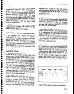
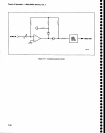
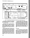
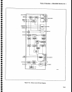
Th€
system in Figure
7-13
depicts a
TV
transmitter
operating
on
Channel
10 with
a video carrier
at
193.25 MHz.
The sideband
adapter
is
tuned
to Channet
10.
The
Spectrum
Analyzer
is
tuned
to 195.25
MHz
with
a span setting
of 1
MHz/Div
(for purposes
of
iilus-
tration,
the
sweep
is
assumed
to
be
halted at
the
center
frequency
of
the
analyzer).
The
sideband adapter
applies
a2MHz
signal
to the
AM modulator
of
the
video
transmitter. Th€ modulator
produces
a lower sideband
at
191 .25 MHz, a carrier
at
193.25
MHz, and an
upper
sideband
at 195.25
MHz.
This signal
is amplified,
filtered,
and combined with
the
FM aural signal.
The
composite signal
is sensed
by
a
RF
pickup
and applied
to th€
RF
Input
ot
the Spectrum
Analyzer.
The 1st
Converter
appli€s
the
composite
signal to
the
'l
st
mixer. The
composite
signal
is
mixed with a
2.26725
GHz
signal
from
the
1st
LO, forming
three
pro-
ducts.
The
subsequent
stages of
the
analyzer accept
onfy
the 2.072
GHz
product
and reject
the
rest. For fre-
quencies
used
in
this example,
the
accepted
product
is
the
difference between
the
1st
LO and
the
upper
side-
band
of
the
TV
signal.
Digital
Control
Circuit
The
digital
control
circuit
provides
the
control
sig_
nals
that select
the
various
Video
Amplifier
functioni.
Addresses
78 and
79
are
decoded
by
U6160
and sent
through
inverter
U6170
as clock
or
enabling
signals
for
gain
latch
u5010
and
mode
tatch
u4010.
Gain latch
lc
u5010
is
an
g-bit
latch
that
suppties
command
data
to
the
8-bit
DAC,
USl
60,
to
offset
the
Log
Amplifier
output
signat.
Mode
tatch
U4O1O
is an
8_
bit
latch
that supplies
command
data
through
the
com-
parators
in
U4020 and
U4160
to select
the
resistors
in
the dB/div switching
circuit
and
to sel€ct
identify, pulse
stretch,
and log
or
linear
mode.
7-35