


Theory
of
Operation
-
494A/494Ap
Servlce, Vol.
1
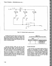
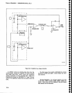
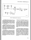
Current
Driver
This
stag€
consists
of
the output
stage
0565/05052;
FETs
Q3061,
eg077,
and
e2074:
amplifiers
U205,4 and
U3054;
and
transistor
e4097.
When
the Preselector
is
not
in
use,
DB2
goes
low and
turns
Q2074 ofi
to reduce
the
coil
current
to zero.
Preamplifier
U2054
reduces
the
temperature
drift of
the output
stage.
Driver
Ofiset adjustment,
R2066 nuils
the
offset
voltage
(at
which
point
the
temperature
drift is
feast).
U2054 drives amptifier
U9054.
A9061 isotates
U3054 from
the
output
driver
Q5052/O565.
Gurrent amplifier
Q5052
drives
the main
preselector
driver
transistor,
Q565.
The
stage
ls
biased so
the
current
divides,
with
most
of
the current
going
through
the
output
transistor. and
a lesser
portion
through
the
bias
circuits.
Th€ curr€nts
rejoin
at
the
preselector
coil.
One set
of
terminals tor
R4049
carries
the coit
current.
the other
set senses
the voltage.
When
th€ DB5 line
goes
low,
the
preselector
is not
swept,
Q4037 and
Q3077
turn on,
which
adds
C4071
across
the Preselector
coil
to reduce
noise
at
the out-
put.
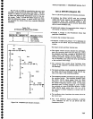
Preselector
Switch
Driver
Operational
amplifier
U10118
and
the complemen-
tary
pair
of
transistors
Q4025/4302S
form
th€
preselec-
tor
switch
driver.
This
circuit
drives
the filter
select
relays shown
on Diagram
12.
The
relays
require
a
posi-
tive
pulse
to select
the
Low-pass
Filter
and
a
negative
pulse
to
select
the
Preselector.
When
the DB4 line
goes
high,
a
positive pulse
of
about
100
ms
in
duration,
generat€d
through RC
differ€ntiator
network
C3021/R302'1,
is
apptied
to
the
input of
ul0118. The
output
of
the operational
amplifier
drops
to
about
-12
V and
a
positive
pulse
is
passed
through
the transistor
pair,
selecting
the Low-
pass
Filter.
When
the DB5
line
goes
low,
a negative
pulse
of
the
same
duration
is
passed
to
U10118. The
amplifier
output
ris6s
to
about
*12
V
and
a negative
pulse
is
passed
through
the transistor
pair
to
select
the
Preselector.
When
the circuit
is
quiescent
neither
e3025 nor
04025 conduct,
since
the sum
of
the zener
voltages ot
VR3011
and
VR3012
is
greater
than
the combined
sup-
ply
voltages.
When
the
output
of
the operational
amplifier
comes
near
one
of
the supply
voltages,
the
transistor,
that is connected
to
the
other
supply,
becomes
saturat€d,
and
supplies
the
drive current
to
actuate
the reiay coil.
CR4012
and
CR4013
protect
the
driver
transistors
from
induced
voltage
surges and
C3028 and
R3028
dampen
oscillation
that
occur in
the
coil.
7-72
CENTER FREOUENCY
CONTROL
(DIAGRAM
35)
The
Center
Frequency
Control
converts
digital infor-
mation, from the front
panel
FREOUENCY
control
or on
the
GPIB
bus, via
the
microcomput€r,
to
analog
vol-
tages for the 1st LO Driver
and Preselector
Driver.
These in
turn
control
the
center
frequency
of
the
analyzer.
The Center Frequency
Gontrol
board contains
ths
tollowing major circuits:
1.
Tha
Digital
Control
circuit,
which buffers and
decodes the
addresses
and other
data to
control
the
other circuits.
2. The coars€ and
fine storage registers
(latch€s),
whibh
store
the
numerical
bytes that
control
the
digital-to-analog
converter
(DAC)
stages.
.
3.
The coarse and fin€
DAC stages, which convert
the digital
inputs
from
the
storage
registers
into
analog curent and voltage
equivalent
values.
4.
The
coarse
and fine
track/hold
amplifiers, which
stor€
the
analog output
values
during th€
approxi-
mation
routine
and compare
the
stored
value
to
the
approximated value for
the microcomputer.
5.
The
write-back
circuits.
which
inform
the micro-
computer when
the
stored
value and th€
approxi-
mat€d valu€s
are
equal.
Operating
Modes
An explanation
of circuit
design
principles
is
giv€n
before
the
operation of
the
circuit
is described.
Two
DAC chips are used in
tandem to
get
the
required reso-
lution. However, this method can cause
errors and
non-monotonic behavior in the overall converter
circuit.
To circumvent this
problem,
the
outputs
of
the tandem
DAC
units
are summed
together
so
that
the two units
are
overlapped
by
three bits.
That is, the
MSB of
the
low-order
DAC
is weighted equally with the third
least
significant
bit,
or
2x10-to
bit
of
the high
order DAC.
The overlap
means
that
the
lower
DAC
will have
sufficient
range
to monotonically
tune the
output of
the
converter over the
entire
range
of
the
analyzer, but
only
if
the
proper
codes of
the lower
DAC device
can
be
found. Now,
suppose
that
the
tandem
DAC
is loaded
as follows:
Upper order
1 0
0 0 0 0 0 0 0 0 0 0
Lower order
111111111111
The contents
ol
the devices
are shown
overlapped
to
illustrate the bit weighting. Now assum€
that the
low-order
device
is
to be
incremented
one
bit.
The
MSB of
the
low-order
device
must
be
moved into the
high-order
device
before the low-order device
can
be
t
o
o
O
I
o
o
o
o
o
I
o
o
o
a
a
a
a
o
I
I
o
o
o
o
o
3
o
o
,
o
I
o
o
a
o
a
o
o
o
o
I
o
t