


a
o
a
o
I
I
o
o
O
o
I
o
o
o
o
a
a
o
o
o
t
t
o
a
a
o
I
o
a
a
o
o
I
o
o
I
a
o
o
o
a
a
I
o
the amplifier.
This
in
turn,
changes
the current
drive
to
the oscillator
coil.
Reference
Supply
- .,
Preamplifier
e2052
plus
amptifie
r lJ20S2
and
emitter
follower
Q2051
,
are
the
active
compon€nts
of
th€
_1
O V
I-ej9fl"":.uppty.
Bias
for
one
sid'E
of
02052
is
set
by
VR1055.
The
other
side.is
set
by
the
_10
V
Adj
R1Og4.
Any
change
in
the suppty
is
amiltiRed
by
e20S2
wnicn
changes
the
drive
to
the
pass
transistoi
eZOSt
*nicf,
compensates
for
the
change.
The
diode
network
across
the
bas€-emitter junction
limits
the
emitter
current
to about
30
mA,
protecting
the
transistor
from
damage.
Mixer
Bias
Driver
The
mixer
bias
driver
circuit,
which
consists
of
quad
IET
switch
U1016,
amptifier
Ul025A,
and
buffer
O202VA1A28,
plus
associated
circuitry,
furnishes
the
required
bias
current (up
to
20
mA)
to
ttre t
st
Mixer
cir-
cuit.
The
bias voltage
varies
from
+1
V
to
_1
V
for
the
internal
mixer,
and
from
+1
V
to
-2.25
V
for an
external
mixer.
External
mixer
bias
voltage
range
can
be
changed
to
-1
to +2.25V
by
moving
the
strap
J2014
from
+12
V
to
the
-12V
suppty.
Mixer
bias
is
selected,
by
the
data
out
of
U4017
to
the
quad
FET
switch
U1016,
and
fed
to
the
inverting
input
of
u1025A.
The
output
of
u1025A
drives
the
base
9f^ 1_Rair
of
complementary
transistors
e102g
and
Q2025
which
provide
the
1st
-ti4ixer
Bias
voltage.
When
any of
the
D0
to D3
lines
from
u4017
go
tow,
the
respective
switch
within
U1016
closes
anld
connects
olg.9!11"
Bias
adjustment
potentiometers
or
the
output
pj.
^U:_0-18
(the programmabte
bias
tine)
to
the
input
of
u1025A.
When
the
D3
output
of
U4017 goes
low,
U1016
selects
the Programmable
Bias
line
ls
the
1st
Mixer
Bias
source.
This
occurs
when
External
Mixer
mode
is
gelectgd.
The
programmable
Bias
is
set
by
the
data
loaded
into
DAC
U9022
!y
the
microcomputei
or
by
the
front
panel
MANUAL
pEAK
controt.
The
MAhiUAL
PEAK
control
is
connect€d
to
the
input
of
U201g
when
the DB4
and
DB7
inputs
to
U4OZ4 go
low
at
address
7E
and
turn
Q3019 on.
When
MANUAL
pEAK
is
setected,
the DAC
output
is
set
for
O V.
Programmable
Bias
When
the microcomputer
sends
address
7E
to
decoder
U4034,
pin
7
(output
7) goes
low.
At
the end
of
deta: output
cycle,
data
is
clocked
into
either
1J4024
or
Ua032,
depending
on
which
latch
is
enabled
by DB6
or
DB7. This
data
is
then
converted
to an
analog
current
Theory
of
Operatlon
-
4g4Al4g4Ap
Servlce,
Vol.
1
by
U3022
which
is
thE
current
sourc€
for
operational
amplifier
U2018.
The
resistance
between
outprrt
termi-
nals
16,
2, and
15 of
U3022
is
th€
input
resistance
for
operationat
amptifier
U2019.
R2022
is
the
feedback
resistance.
The
output
of
U20lg
is a
bias
voltage
that
is
fed,
via
the Programmable
Bias
line,
to either
the
Presel€ctor
Driver
board
where
it
is summed
with
the
drive
voltage
for
the
preselector;
or,
it
is
fed
through
U1016/U1025A,
and
e1028/e2025
to
the
829Mfr2
Diplexer,
then
through
the
Transfer
Switch
on
the
RF
deck
to the
External
Mixer port.
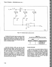
PRESELECTOR
DRIVER
(Diagram
34)
The
Preselector provides
RF
input
selectivity
between
7.7
and 21
GHz. This
selectivity
reducei
spurious
responses
over
this frequency
range.
The
Preselector
Driver
supplies
the
drive
iurrent
to
the
Pr€selector
coil
(shown
on
Diagram
12)
to tun6
the
Preselector.
lt also
furnishes
a
voltage
that is
propor_
t]o_B!
t9 frequency
change
through
the rear-panel
ACCESSORIES
connector
for
an external
preselecior,
if
used. The
circuit also
operates
the filter
select
relay
that selects
either
the
pr€selector
or
Low-pass
Filtei.
The
major circuits
and
their
functions
are:
.
The
digital control
circuit,
which
stores
and
decodes
the
data
from
the microcomputer
and
con-
trols
the
other
circuits
within
the
preselector
Driver.
The
digitat
controt
circuit
appties
the
spAN voLTS
signal
to
the
oscillator
voltage
processor
when
FM
coil
spans
are
selected,
selects
the
gain
of
the
oscillator
voltage
processor,
turns off
the
drive
sig_
nal
to
lhe
curr€nt
driver
for
degauss cycles
or
when
the
preselector
is
not
in
use, selects
the
lF offset
voltages
to
be combined
with
the
FINE
TUNE
VOLTS
signaf,
adds
noise
filtering
at
the
driver
out-
put
when
th€
preselector
is
not
being swept,
and
controls
the filter select
switch.
r
The oscillator
voltage processor,
which
attgnuates
and
offsets
the input
signal
for application
to
the
summing
amplifi€r.
o
The lF offset
stage,
which
applies
an
offset
voltage
to
the summing
amplifier.
.This
offset
is
propor-
tional
to the 1st
lF
frequency
in
use, including
the
effects
of
fine
tuning
frequency
changes
of
the 2nd
Local
Oscillator.
e
The
summing
amplifier.
which
combines
the
effective
oscillator
frequency
voltage
and
the
lF
Offset
voltage
to
drive
the tracking
adjustment cir-
cu,ts.
7-69