


a
o
o
I
o
I
o
I
o
o
o
I
o
o
o
O
a
a
o
o
o
O
o
o
o
o
a
o
I
o
a
o
I
a
O
o
o
o
a
o
I
a
I
a
Calibrator
u2022
and
related
components
regulat€
a
100
MHz
signat
to
-20dBm
for
the
front-panet
ill
bUf
connec_
tor.
VRI
0S1
serves
as
an
aecurate
6.2
V
reference,
which
is
divided
to approximately
1.e
V
anO
applied
to
pin
6
of
U2022.
The
exact
tevet
ii
set
by
R1041
the
Cal
Level
adjustmsnt.
The
100
MHz
signal_
enters
pin
1 and
passes
through
a
pin
diode
variable
attenuator.
The
signal
is
th€n amptified
and
passed
through
a
low-pass
fitter
to
remove
any
harmonics.
The
signal
then
enters
a
peak
detector-
and
comparator
wnere
the
peak
amplitude
of
the
100
MHz
signal
is
compared
to
the
1.2
V
reference
on
pin
6. An
operational
amplifier
then
adiusts
the
att€nuation
level
of
the
pin
dlode
to
maintain
a constant
signat
level.
The
outqq
of
this
operationai
ampliRer
can
be measured
on
Tp301l.
A
small
fortion
of
the
1^0-0
MHz
signal
is
attenuated
tnrou'gh
RzO.ll
to
-20dBm.
R1021
and
R1022
suppfy
Uia-s-current
to the
p€ak
detector
circuits.
fne
vottale
on
pins
7
and
g
should
typicaily
be +5
V.
c2023,
C2011,
and
related
components
form
a
high-pass
filter
to allow
harmonics
of
iOO
Mn.
to
pass
through
to the
front
panet.
The
nna
resutt
is
a
calibra-
tor signal
rich
in
harmonics
with
an
accurate
100
MHz
amplitude.
In
Option
0Z instrum€nts,
the
CAL
OUT
signal
goes
thr:ugh
a
set
of-relay
switches.
tn
50O
moOe,
the out_
put
goes
straight
to
the
CAL
OUT
connector.
In
the
750.mode,
the output
is routed
through
a
50O_to-ZsO
matching pad
and
the
output
is
+ZO
Og-mV.
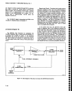
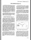
REFERENCE
LOCK
(Diagram
S0)
The
Reference
Lock
module
(A36)
consists
of
a
".tlblg
10
MHz
crystat
osciilator
'(A3erc),
reference
detector,
frequency
.synchronizer,
phaie/frequency
detector,
and
tune
window
detector.
Eittrer
tne
internal
10
MHz
reference
or
an
external
1,2,5,
or
10
MHz
refer-
ence
frequency
is routed
through
the
reference
detector
1o-^tlg -frequency
synchronizer.
The
local
oscillator,s
100
MHz
output
is
divided
by 100
and
apptied
to one
inp.ut
-of
a
pha.se/frequency
dbtector
wtrich'tompares
it
with
the
i
MHz
reference
frequency.
Th€
resultant
error
signal
is
amplified
by
the
tune
amplifier
and
applied,
as
a
corrective
voltage,
to
the
voltage
con_
trolled
3rd LO.
Theory
of
Operation
-
4g4Ll4g4Ap
Service,
Vot.
1
External
Reference
Detector
_
Buffer
amplilier
02014
converts
Extemal
Reference
signals,
within
the
range
of
-iS
dBm
to +15
dBm,
into
TTL
compatible
level.
When
an
ext€mal
signal,
within
!!e tgvet
rangE,
is
apptied,
it
triggers
muttivibrator
U20468.
.
The
output
of
U2046B
enaOles
ext€rnat
signat
control
NAND gate
U20g2D,
and
disables
the inte-rnal
signal
control gate
U2032A.
lt also
disables
the internal
10
MHz referEnce
osciltator
by
turning
el0g1
on,
which
biases
Q1033 off,
and
r€moves
the
+5
V"
supply
for
the
osciltator.
The
output
of
U20468, pin
9i
is
sent
to the
processor,
on
the
EXT
REF
line,
to
indicate
that
an
external
reference
frequency
is
in
use.
During
a
diag_
nostic
test,
the microprocessor
can
also
pult
the
INTEi_
NAL
SHUT-DOWN
line
down
to
turn
the
lnternat
Refer-
ence
Oscillator
off
and
check
for
loop
unlock.
lJ2Og2B
gates
either
the
10
MHz
from
the internal gate
u2o32A,
or
the
external
reference
from
ltZOgZD,
to
ihe frequency
synchronizer
U2046A.
Frequency
Synchronizer
Multivibrator
U2046A,
synchronizes
its
1
MHz output
with
any of
the allowed
input
frsquencies
by edge_
triggering
the time-out period.
The
I MHz
ouiput
fre-
quency
is set
by
the timing
components
R2039,
c2o3g,
and
adjustment
R2042.
With
a
10
MHz signat
applied
to
U2046A,
adjustrnent
RZO4Z
is set
for
a
lrrs
period,
with
65 ns
between
the
falling
edge
at
Tp2046
and
the
next
falling
edge
at
Tpl044.
Phase/Frequency
Detector
The
100
MHz
from
the
3rd Local
Oscillator
is
clivided
by 100
and
converted
to a TTL
level
by
pres-
caler
U2020.
The
I MHz
from
U2020,
is
fed
to
the
clock
input
of D-type
flip-flop
U1O44A.
The
1 MHz
from
U2946A,
is
applied
to the
clock input
of D-type
flip-flop
U10448.
The
two
ftip-flops
and
NAND
gaie
UZOO2C,
form
the Phase/Frequency
Detector.
R1Og4,
Rl0gS,
and
C1037, along
with it's
counterpart,
on
the output
of
U1044A,
form
a low-pass
averaging
filter for
the outputs
of
the
flip-flops.
When
the
two input
frequencies
are
equal
and
in
phase,
the
composite
output of
the averag-
ing
filter
is +2.5
Vdc.
7-21