


o
o
o
t
o
o
o
I
o
O
o
I
o
o
a
o
o
a
t
o
o
o
o
o
o
o
a
o
I
o
I
o
t
o
o
o
o
I
o
o
I
o
t
a
Theory
of
Operation
_
4g4Al4g4Ap
Service,
Vol.
1
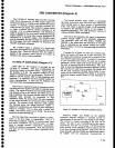
3RD
CONVERTER
(Diagram
4)
The
1t0MHz
tF
Amptifier
(A32)
and
3rd
Converter
(A34)
down
converts
the
ttO
MHz
ouiput
signat
from
the
2nd
Converter
to 10
MHz
for
the
VariaUie
Resolution
circuits.
A
100
MHz
crystat
controlled
oscillator
pro-
vides.the
third
LO
signal.
This
oscillator
is
phase
locked
to either
a
precise
internal
10MHz
reference
or
an
external
1,
Z,
5, or
10
MHz
reference.
The
100
MHz
LO
signar
is
applied
to
the
mixer
and
is
oistriouteo
through
output
amplifiers
to
many
other
circuits
throughout
t6e
instrument
as
a reference
signal.
The
100
MFz
signal
and
its
harmonics
are
also
available
for
external
use
at
the front-panel
CAL
OUT
connector
for
irequency
anO
100
MHz
amplitude
calibration.
.
The
110
MHz
signal
is
amplified
in
a
three_stage
gain
btock
and
apptied
through
a
band_pais
fitter
and
a
low-pass
fitter.
From
the
toiv_pass
fil6r,
the signal
is
applied
to
the converter,
which
consists
of
a
mixer,
an
oscillator,
and
various
output
amplifiers.
110
MHz
tF
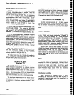
AMpLtFtER
(Diagram
17)
-lnitial
gain
for
the analyzer
is
provided
by
the
110
MHz
lF
Amplifier.
Thi;
gain
compensates
for
conversion
losses
in
the
thre€
mixers.
Typical
gain
for
the amptifier
is
2t
dB.
The
amplifie,
"onjirts
of
three
stages
of
amplification
and
an
attenuator.
The
first
two
mixers
in
the
RF
syst€m
ofier
no
high_frequency
gain;
therefore,
it is
important
that
this
ariptifiei
exhibit
low
noise
characteristics.
lt
must
atso
be relatively
free
from
third-order
intermodulation
distortion.
.
Signal
input
is
applied
through
an
impedance
rnatch-
ing
b.and-pass
fitter
(L2044
anO
CSZS)
to'a
parailel
tuned
circuit.
The
signal
is injected
into
the
paraltet-tuned
cir_
cuit
through
a
tap
in
the
inductor
and
taken
out
at
the
high
impedance
side
through
variable
capacitor
f;2A47.
Inductive
input provides
for
"onu"riion
to
high
impedance
within
the
tuned
circuit;
the
extra
capacltor
on
the output provides
for
conversion
back
to 50 ohms
l.Iil_"]:_I!:
pr'.m."ry.
tuning
capacitor,
C325,
adjusts
tn€ resonant
point;
the
output
capacitor,
C20C7,
is
adjust€d
in combination
with
bSZS
t6r
good
impedance
match
at
110MHz.
This
is
done
wiih
a
return
loss
bridge.
The
nominal
return
loss
is
35
dB.
The
e of
the
input
filter
is approximately
20.
-
From
the input
fitter,
the
signat
is
applied
to
e4053,
which
is
the
first
stage
of
impliRcaiion.
This
is
a
broad-band
feedback
amplifier
to
provide
good
input
and
output
impedance
and
controlied
gain.
All
feed-
919!
is
through
reactive
componenti
(transformer
T3054),
not
resistive
cornponents.
Thus,
the
impedance
and
gain
can
be controlled
without
significant
noise
problems.
..
The
second
amplifier
stage,
e40g7,
is
essentially
the
same
as
the first,
with
oniy
minor
bias
differences.
Gain
through
each
of
these
itages
is
approximately
9
dB. The
output
is
applied
through
a
3
dB
attenuator,
to..preserve
the impedance
figure,
to
the
bridged
.T;
adjustable
attenuator.
The
3
dB attenuator
consists
of
resistors
R2039,
R2038,
and
R2043.
From
the
3 dB attenuator,
the signal
is
capacitively
goupled
through
C2Ogl
to
the aOyustabte
attenuator.
This
attenuator
uses
two
ptN
diodes,
CR3030
and
CR1029,
in
the
mode
when
the
resistance
to
RF
signal
lolv
is c_ontrolled
by
the
current
through
the
diodes.
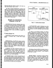
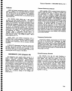
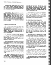
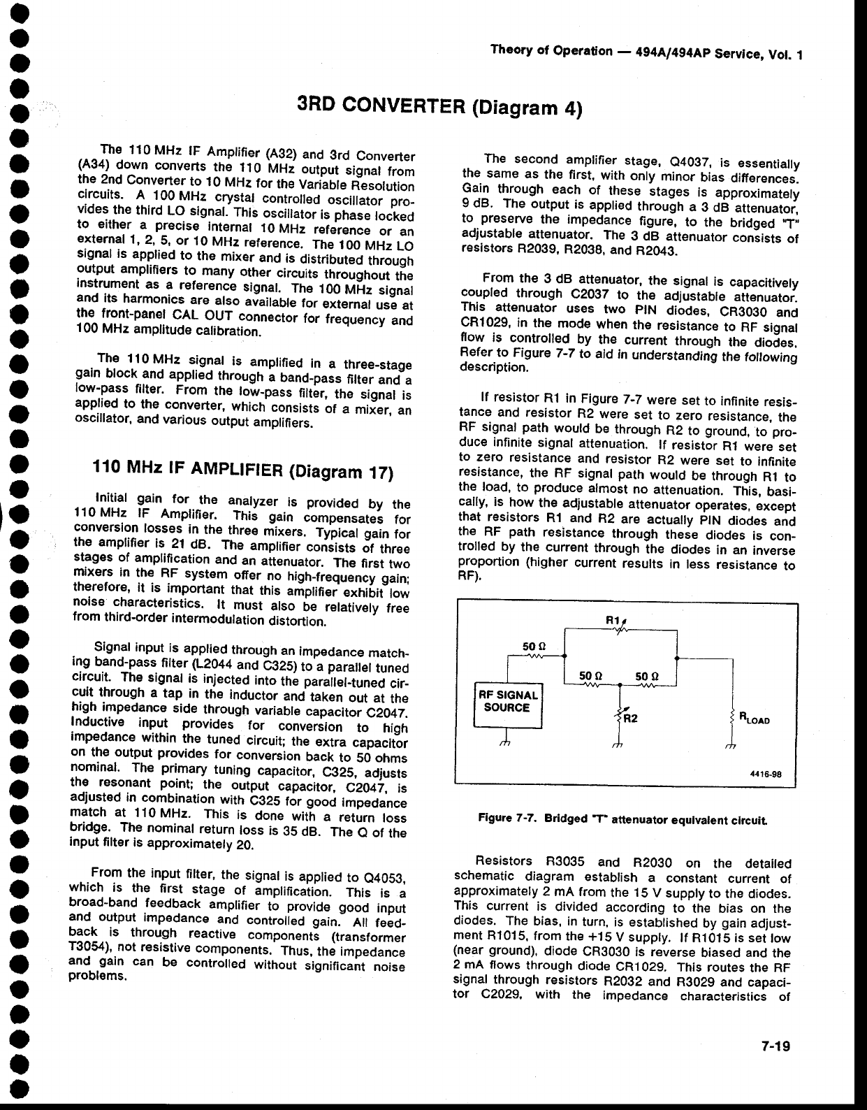
Refer
to
Figure
T-7
to aid
in
understandirig
tt e
foflowing
description.
f f
resistor
R1 in
Figure
7-T
were
set
to infinite
resis_
tance
and resistor
R2
were
set
to zero
resistance,
the
RF signal path
would
be
through
R2
to
ground,
to
pro-
duce infinite
signal
attenuation.
lf
resistor
Rl were
set
to
zero
resistance
and
resistor
R2
were
set
to infinite
resistance,
the RF
signal path
would
be through
Rl
to
th€ load,
to
produce
almost
no
attenuation.
This,
basi-
cally,
is.how
the
adjustable
attenuator
operates,
except
that resistors
R1 and
RZ
are actually
plN
diodes
and
the
RF
path
resistance
through
theie
diodes
is
con-
trolled
by
the
current
through
the diodes
in an
inverse
proportion
(higher
current
results
in
less
resistance
to
RF).
Figute
7-7.
Bridged
'T'
attenuator
equlvalent
clrcuit
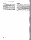
Resistors
R3035
and
R20gO
on
the detail€d
schematic
diagram
establish
a
constant
current
of
approximately
2
mA from
the
15
V supply
to the diodes.
This
current
is
divided
according
to
the bias
on
the
diodes.
The
bias, in
turn,
is established
by
gain
adjust-
ment
R1015,
from
the
+15
V suppty.
lf Rl015 is set
low
(near
ground),
diode
CR30g0
is reverse
biased
and
the
2 mA
flows
through
diode
CR1
029.
This routes
the
RF
signaf
through
resistors
R2092
and
R3029
and capaci_
tor C2029,
with
the
impedance
characteristics
of
7-1
9