Appendix A: Options and Accessories
AWG2021 User Manual
AĆ11
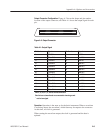
Table AĆ2: Connector Pin Assignments (Cont.)
Pin Number SignalPin NumberSignal
9 D4 23 D11 (MSB)
11 D5 25 Clock
13 D6
Pins other than those mentioned are connected to ground. The pin assignments
are identical for both CH1 and CH2.
H Operation. Operation is the same as for the basic instrument. When a
waveform is not being output, the waveform’s initial data may be output to
the connector. At this time, no clock is generated.
When starting the waveform output, the clock is generated and the data is
updated.
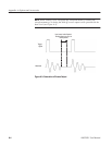
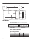
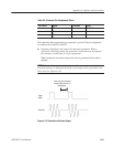
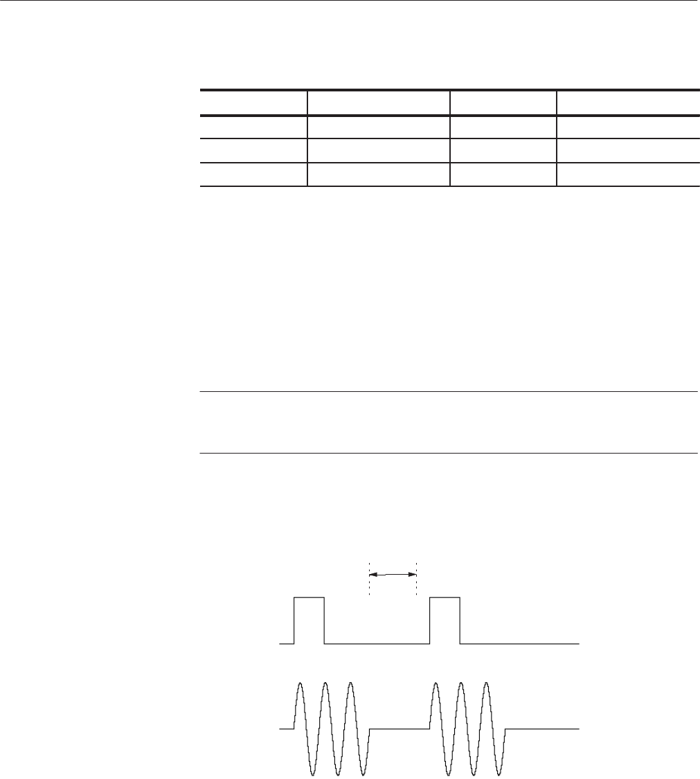
NOTE. When loading a new waveform into waveform memory, resetting the
waveform memory, or during the hold off, excess output can be generated in the
data clock (see Figure A-12).
Trigger
Signal
Waveform
these periods.
Load, reset, holdĆoff period:
Excess output can occur in
Figure AĆ12: Generation of Excess Output


