Appendix E: Functional Operation Summary
EĆ10
AWG2021 User Manual
Waveform
Memory
Clock (1/8)
Length
Counter
Address
Counter
Looping
Counter
Sequence Memory
Address Counter
Sequence Memory
AAA WFM
Address
AAA WFM Data
Length
Looping Control
Value
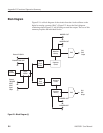
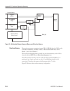
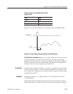
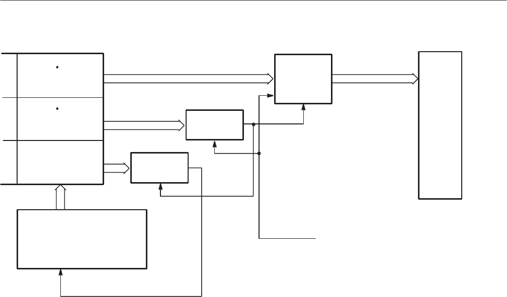
Figure EĆ9: Relationship Between Sequence Memory and Waveform Memory
The waveform memory comprises sixteen 32K 8 SRAM chips for 256K words
of 16-bit word memory. Of these 16 bits, 12 bits are waveform data, 1 bit is
Marker 1, and 1 bit is Marker 2
The waveform and marker data is loaded into waveform memory when a file is
selected with the SETUP menu Waveform Sequence item.
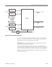
Since the waveform memory must be read out at high speed (250 MS/s), it is
partitioned into 8 banks and read out with 8:1 multiplexing (parallel-serial
conversion). Therefore, the memory itself operates with a
1
/
8
clock.
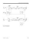
Figure E-10 shows the waveform memory configuration.
Waveform Memory


