


SA-1110 Developer’s Manual 107
System Control Module
• Type 7 – These pins are inputs and are actively sampled during sleep.
• Type 8 – These pins are inputs and are not observed during sleep; the receiver is disabled.
• Type 9 – These pins are analog inputs and outputs, and are always active.
9.5.7 Power Manager Registers
The power manager is controlled through eight 32-bit registers. The power manager control
register (PMCR) is used to allow software invocation of sleep mode. The sleep status register
(PSSR) contains status bits that indicate why sleep mode was invoked. The power manager scratch
pad register (PSPR) is a general-purpose register used to store processor data during sleep. The
power manager wake-up enable register (PWER) is used to program the desired wake-up sources
in the system. The power manager general configuration register (PCFR) contains bits used to
control various configurable functions within the SA-1110. The power manager PLL configuration
register (PPCR) allows the user to change the PLL operating frequency. The power manager GPIO
sleep state register (PGSR) is used to program the value loaded onto GPIO outputs when the
SA-1110 transitions into sleep mode. The power manager oscillator status register (POSR) contains
a single bit that indicates whether the 32.768-kHz oscillator has stabilized after a hardware reset.
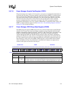
9.5.7.1 Power Manager Control Register (PMCR)
Sleep mode is invoked by setting the force bit within the power manager control register (PMCR).
The force bit is automatically cleared upon exiting sleep mode or when a hardware reset occurs.
Writing zero to the force bit has no effect. For reserved bits, writes are ignored and reads return
zero. This register should be protected by programming MMU permissions. The following table
shows the PMCR.
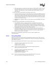
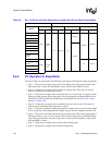
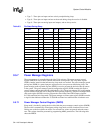
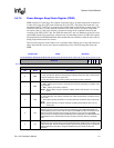
Table 9-3. Pin State During Sleep
Pin Name Type Pin Name Type Pin Name Type Pin Name Type
A[25:0] 1b nPIOR 2 UDC- — VDD_FAULT 7
D[31:0] 1b nPCE[2:1] 2 TXD_1 4 nRESET 7
nCS[5:0] 2 nIOIS16 8 RXD_1 4 nRESET_OUT 1b
RDY 8 nPWAIT 8 TXD_2 4 nTRST 8
nOE 2 PSKTSEL 1b RXD_2 4 TDI 8
nWE 2 nPREG 1b TXD_3 4 TDO 6
nRAS/nSDCS[3:0] 1 L_DD[7:0] 4 RXD_3 4 TMS 8
nCAS/DQM[3:0] 1 L_FCLK 4 GP[27:0] 3 TCK 8
nSDRAS 2b L_LCLK 4 SMROM_EN 8 TCK_BYP 7
nSDCAS 2b L_PCLK 4 ROM_SEL 8 TESTCLK 7
nSDCKE[1:0] 1b L_BIAS 4 PXTAL 9 VDD —
nSDCLK[2:0] 1b TXD_C 4 PEXTAL 9 VDDX —
RD/nWR 1b RXD_C 4 TXTAL 9 VSS —
nPOE 2 SCLK_C 4 TEXTAL 9 VSSX —
nPWE 2 SFRM_C 4 PWR_EN 5 ——
nPIOW 2 UDC+ — BATT_FAULT 7 ——