


SA-1110 Developer’s Manual 141
Memory and PC-Card Control Module
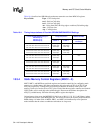
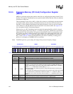
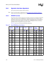
Bits Name Description
1..0 RTx 1..0
ROM type timings.
00 – Nonburst ROM or Flash memory.
01 – Nonburst ROM or SRAM for nCS[2:0] variable latency I/O for nCS[5:3].
10 – Burst-of-four ROM or Flash (with nonburst writes).
11 – Burst-of-eight ROM or Flash (with nonburst writes).
All four ROM timings support read bursts of any allowable burst length (number of burst
beats). Burst-of-four and burst-of-eight timings refer to the use of read bursts where modulo
four or eight addresses within a burst require the same access times as nonburst reads,
but shorter access times are allowed for each non-modulo four or non-modulo eight beat
within the burst. Read bursts are always address aligned to their burst length.
The data size of writes to types 00, 10, and 11 must always be less than or equal to the
width of the corresponding external data bus: no larger than a single 32-bit word write to a
32-bit data bus, and no larger than a 16-bit half-word write to a 16-bit data bus. Unexpected
results, including data loss or corruption, may occur if larger data size writes are attempted.
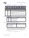
2RBWx
ROM bus width.
0 – 32 bits
1 – 16 bits
On hardware or sleep reset, the RBW0 field in MSC0 is loaded with the inverse of the
ROM_SEL pin. It can be subsequently overwritten.
RBWx bits must remain clear if the corresponding chip selects are configured for
Synchronous Mask ROM (SMROM). Also, if nCS 0 is configured for SMROM by holding
the SMROM_EN pin high during hardware or sleep reset, the ROM_SEL pin must be held
high. See Section 10.4 for details on SMROM configuration.
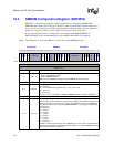
7..3 RDFx 4..0
ROM delay first access.
Number of memory clock cycles (minus 2) from address to data valid for first read access
to nonburst ROM or Flash, burst ROM or Flash, or SRAM. Also, the number of memory
clock cycles (minus 1) from address to data valid for subsequent read accesses to
nonburst ROM or Flash, or SRAM; and the number of memory clock cycles (minus 1) of
nWE assertion for write accesses (nonburst) to burst Flash.
For nCS[5:3] variable latency I/O, this determines the minimum number of memory clock
cycles (minus 1) of nOE (nWE) assert time for each beat of burst read (write).
12..8 RDNx 4..0
ROM delay next access.
Number of memory clock cycles (minus 1) from address to data valid for subsequent
accesses to burst ROM or Flash. Also, the number of memory clock cycles (minus 1) of
nWE assertion for write accesses to nonburst Flash or SRAM.
For nCS[5:] variable latency I/O, this determines the minimum number of memory clock
cycles (minus 1) of nOE (nWE) deassert time between each beat of burst read (write).
15..13 RRRx 2..0
ROM/SRAM recovery time.
Number of memory clock cycles (divided by 2) from chip select deasserted after a read to
next chip select (of a different memory bank) or nRAS/nSDCS asserted.
For Flash, SRAM, and nCS[5:3] variable latency I/O this field will also be used after writes
to hold off subsequent accesses.
This field should be programmed with the maximum of Toff, write pulse high time
(Flash/SRAM), and write recovery before read (Flash).
If the system is also configured for SDRAM or SMROM using auto-power-down (see
Section 10.3.2), This field must be non-zero to ensure proper auto-power-up behavior for
SDRAM or SMROM accesses that follow accesses to this static memory bank. However, the
recovery time between SRAM accesses must be set to satisfy the minimum
nCAS/DQM[3:0] deassertion time for any asynchronous DRAM present in the system.