


358 SA-1110 Developer’s Manual
Peripheral Control Module
11.12.5.3 MCP Data Register 2
MCDR2 contains 21 bits and is used to perform reads and writes to any of the UCB1x00’s
registers. MCDR2 contains three separate fields: MCDR2[15:0] is the 16-bit register data field,
MCDR2 16 is a 1-bit read/write control bit, and MCDR2[20:17] is the 4-bit register address field.
A value written to MCDR2 is placed in the correct position within the 64-bit subframe 0, is
transmitted to the off-chip codec, and is used to perform a read or write operation to the addressed
codec register. Note that the contents of the addressed register are always returned in the receive
data frame and placed in the MCDR2 regardless of the state of the read/write bit. Thus for write
cycles, both a write and a read occurs, and for read cycles, only a read occurs. When MCDR2 is
read, the value returned from the last read or write operation, which was completed to the codec, is
returned.
A register write is performed by writing the correct value to each of the three fields within MCDR2
using one 16- or 32-bit write, ensuring that the read/write bit is set. Its contents are then transferred
to the correct fields within the serial shifter on the next rising edge of the SFRM signal, and then to
the codec via the TXD4 pin during subframe 0. The value within MCDR2[15:0] is written to the
selected codec register at the end of subframe 0 (during the 65th bit of the frame). The data written
to the control register and its address is returned to the MCP during the next data frame, and is
placed back within MCDR2 with the read/write bit reset to zero. For a write operation, since the
addressed register is written at the end of subframe 0, the data returned during the frame in which
the write occurred represents the previous contents of the register. The updated value is returned
during the next data frame.
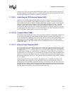
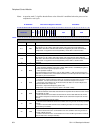
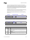
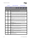
0h 8006 000C MCP Data Register 1: MCDR1 Read/Write
31 30 29 28 27 26 25 24 23 22 21 20 19 18 17 16 15 14 13 12 11 10 9 8 7 6 5 4 3 2 1 0
Reserved
Bottom of Telecom Receive FIFO
Reset
0 0 0 0 0 0 0 0 0 0 0 0 0 0 0 0 0 0 0 0 0 0 0 0 0 0 0 0 0 0 0 0
Read Access
31 30 29 28 27 26 25 24 23 22 21 20 19 18 17 16 15 14 13 12 11 10 9 8 7 6 5 4 3 2 1 0
Reserved
Top of Telecom Transmit FIFO
Reset
0 0 0 0 0 0 0 0 0 0 0 0 0 0 0 0 0 0 0 0 0 0 0 0 0 0 0 0 0 0 0 0
Write Access
Bits Name Description
15..0 Telecom Data
Transmit/receive telecom FIFO data.
Read – Bottom of telecom receive FIFO data.
Write – Top of telecom transmit FIFO data.
31..16 — Reserved.